Continue to Site

Welcome to EDAboard.com

Welcome to our site! EDAboard.com is an international Electronics Discussion Forum focused on EDA software, circuits, schematics, books, theory, papers, asic, pld, 8051, DSP, Network, RF, Analog Design, PCB, Service Manuals... and a whole lot more! To participate you need to register. Registration is free. Click here to register now.

logic of pulse input of a buffer for PDN analysis

yefj

Advanced Member level 4
Joined
Sep 12, 2019
Messages
1,192
Helped
1
Reputation
2
Reaction score
3
Trophy points
38
Activity points
7,199
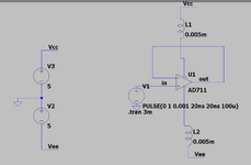
Hello , I have a pulse signal going into a buffer, L1 and L2 represent bad PCB power delivery network to this buffer.
the goal of a good PDN network that we will not have HIGH impedance between Vcc and GND.
sudden change of input can cause sudden change of DC current consumption.
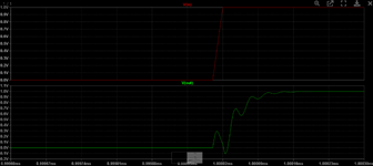
i want to improve the situation so my pulse signal with pass without destortions shown bellow.
I know i need to plan the PDN according to the impedance profile at some frequency range.
I know my pulse can be viewed at frequency responce usint FFT.
Could you please say at what frequency range i need to plan my PDN?
Thanks.

1699023436262.png


1699023395370.png
 

Attachments

  • 1699023409732.png
    1699023409732.png
    71.1 KB · Views: 45
  • 1699023409561.png
    1699023409561.png
    266.7 KB · Views: 40
  • 1699023411850.png
    1699023411850.png
    71.1 KB · Views: 44
Your step response appears to oscillate near 40MHz with a rise time near 3 cycles. The schematic inductance implies the load capacitance in the range of a 3.3 pF. The AD711 has a nom. BW of 3 MHz and a slew rate of 20V/us. Thus we see the output is slew rate limited which means it is output current limited, rated for 25 mA nom.

Looking at the AD711 specs, the open loop, the TPC 3 shows the 50% output swing or output impedance to be about 300 ohms.

Your question assumes driver impedance has some high impedance transition is the speed limitation for digital pulses.
> "the goal of a good PDN network that we will not have HIGH impedance between Vcc and GND."..."Could you please say at what frequency range i need to plan my PDN?"

- Although negative feedback lowers the output Zo with gain, it does not at -3 dB BW nor at max slew rate.

- The resonance in your simulation implies only a load capacitance of 3.3 pF for 10 uH.
- One must try to avoid mis-matched impedance reflections is to match the source impedance to the path
- discontinuities in source impedance need to be attenuated by the slew rate limit over a small percentage of the swing. Bipolar OA drivers at max slew rate will rely on internal negative feedback for current limiting. Knowing current sources are high impedance supports your assumption that there is a high impedance state during the transition.

Suggestions

Lowering the Vcc-Gnd-Vee impedance with shunt caps across the device will raise the SRF frequency as suggested in the datasheet schematics.

The shunt capacitor of 0.1 uF is typically used which has a self-resonant frequency > 40 MHz.

The other method of reducing supply or signal ripple where PSRR is poor at HF, is to use a series RC filter for each Vcc,Vee with a tolerable voltage drop.
However your simulation has more ripple than spec. plot TPC 23c step response which is curious.
 
Hello,actually my goal is to test the pulse responce to the QPA2575 amplifier.i dont have spice model of the QPA2575
I have used this OP-AMP buffer configuration model as an alternative.
few questions:
1.do you think that is a good altenative?
2.could you please reccomend me some other model which could be better based on the data sheet of the device?
my goal is to optimise the power delivery network surrounding the QPA2575 amplifier.
and to test the pulse respoce with PDN s-param extractions instead of the inductor i put in the ltspice model.

 
Hello,my system is as shown bellow.
PDN could be with high impedance and ruin the voltage suply to the QPA2575.
how do i know at what frequency range i need to plan my PDN ?
So my output signal will not be destored by a problematic PDN.
maybe it has something to do with frequency represntation of the pulse?
Thanks.

1699041909285.png
 
Series inductance of 5 uH looks like an intentional bad power supply. Realistically it won't be seen in a real PCB without additional bypass elements. The waveforms obtained with this PDN can be considered as "garbage in - garbage out".

The specific simulation results aren't necessarily reliable, SPICE models have limited validity beyond regular operation conditions. Hopefully, common mode rejection is modeled, supply pin impedance less likely.

No big problem to achieve supply |Z| < 1 ohm or even 0.1 ohm over the operation frequency range instead of 1 kOhm @ 30 MHz in your circuit.
 
Hello FVM ,so what frequency range do i need to focus on ?
Thanks.
 
Last edited:
UPDATE:
Hello i got it all wrong.based on the data sheet. the pulse is from Vcc not Vg.
i have done FFT to the impulse written in the data sheet shown below.

based on the FFT to what frequency range do i need to design my PDN?
Thanks.
1699089027894.png


1699088243038.png

1699088822330.png

1699088849776.png


1699088909871.png
 
Last edited:
Hello Tony , i have some RF input but we modulate using the Vd bias.
Low impedance means that there will be no large voltage drop and we will get as close as possible to 6 volts.as you said in your good advice our amplifier is just a 6/2.1~3Ohm load
I have built an AC input impedance response of the network of the data sheet plus 3 ohm load for amplifier as shown below.

did i represent correctly the PDN?
Thanks.

1699110558235.png

1699111528188.png


1699110677522.png

1699111424227.png
1699111409432.png
 
Hello,i do have a contradiction regarding the purpuse of a PDN.
1.on one hand i know the theory that if a line is too inductive than its a problem because in high frequency this means high impedance.
and there will be big voltage drop and not enough voltage will be on the device.
so if we put Vd as a pulse form 0 to 6V and 20nsec rise time then i will not happen and we need to put capicitors to make this pulse to pass more smoothly.
the problem with this concept that FFT of a pulse is endless as shown bellow,so i dont know the frequency range i need to plan my PDN?

2. The PDN use decoupling/bypass capacitors so that high frequency noise will not go to the device but to the ground.
this concept is tottaly different from concept 1 beacuse if i filter high frequency noise then i could by accident to filter the harmonics of the pulse.

So if you could please show the logic which could unite these two concepts.
Thanks.

1699164334739.png
 
Hello FVM ,so what frequency range do i need to focus on ?
E.g. 0 - 50 MHz.
--- Updated ---

To model PDN meaningfully, it's necessary to include power source and trace impedance. Post #10 schematic obviously can't serve this purpose.

Regarding post #1 buffer schematic, I don't think that it makes much sense to perform a simulation without load.
 

LaTeX Commands Quick-Menu:

Part and Inventory Search

Welcome to EDABoard.com

Sponsor

Back
Top