Continue to Site

Welcome to EDAboard.com

Welcome to our site! EDAboard.com is an international Electronics Discussion Forum focused on EDA software, circuits, schematics, books, theory, papers, asic, pld, 8051, DSP, Network, RF, Analog Design, PCB, Service Manuals... and a whole lot more! To participate you need to register. Registration is free. Click here to register now.

[SOLVED] CSt WMS: Circular Waveguide - How to interpret the simulation result ?

Status
Not open for further replies.
A

aveore

Guest
CST MWS: Circular Waveguide - How to interpret the simulation result ?

Hi,
[With what software does the given design is based on: CST Studio Suite 2012/CST Microwave Studio 2012]

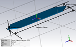
I have build a circular waveguide with tapered extruded sections at each ends of the waveguide. I have also successfully simulated the design with 1 or 2 warnings and got results as well, but not quite sure of understanding the simulation results. Could somebody help me to interpret the S-parameter (magnitude vs frequency) outputs of this waveguide. I have attached a pdf file of my design with respective simulation result in it. Below is some specificatrion of my design (if in case somebody need it).

Design Specification:

  • Frequency Range: 8GHz - 12Ghz
  • Material Used : Aluminum [Type: lossy metal]
  • Boundary Condition: Xmin & Ymin = Conducting wall, Zmin = open (add space)
  • Field Monitors : E-field [Fmin=8 GHz, Freq=10Ghz, Fmax=12Ghz]
  • Solver: Time domain [Mesh type=Hexahedral, Accuracy=-40dB]
Look for the attached .pdf file for full details of the design. Please help me guys, I need this for a crucial part of my dissertation.

Regards,
Aveore
 

Attachments

  • Results.pdf
    1.3 MB · Views: 166
Last edited:

Re: CST MWS: Circular Waveguide - How to interpret the simulation result ?

Hi
Which boundary conditions did you set for Xmax, Ymax and Zmax?
 

Re: CST MWS: Circular Waveguide - How to interpret the simulation result ?

Thank you for the reply, I have used "open (add space)" for all Xmax, Ymax and Zmax. I have touched nothing else in the boundary condition.

**EDIT**
I have just shown my graphs to my professor and he's ok with these magnitude graphs for the waveguide with I provided here. He now asks me to plot graphs for phase shift. I on the other end got no idea of how to do get a phase shift graph. I am using a tapered rectangular dielectric slab in the waveguide both in vertical and horizontal position. So, he needs to see the phase shifts for both positions and compare them to see if they both are 90 deg to each other.


Help me with this issue now please. I have attached my Dielectric slab design screenshots here. Kindly see them and enlighted me.


Dielectric Slab Specs:
Y-axis -> height = 1.0mm
X-axis -> width = 21.5mm
Z-axis -> length = 73mm

Screenshots:
Front view of both horizontal and vertical dielectric slabs in the waveguide

Front view of the Horizontal dielectric slab in the waveguide.PNGFront view of the Vertical dielectric slab in the waveguide.PNG

Side view of the vertical dielectric slab in the waveguide:
Side view of the vertical slab in the waveguide.PNG


Top view of the horizontal dielectric slab in the waveguide:
Top view of the horizontal slab in the waveguide.PNG
 

Attachments

  • Dielectric Slab.png
    Dielectric Slab.png
    28.3 KB · Views: 178
Last edited:

Thanks for at lease viewing my post guys. I have figured out why I wasn't getting the phase shift. I forgot to enable the "Polarization Angle". My bad. If anybody is curious to see what I am talking about, just click the pic.

This post may be useful for future students, so I will leave all the attachments.

Polarizartion Angle.PNG
 

Status
Not open for further replies.

Similar threads

Part and Inventory Search

Welcome to EDABoard.com

Sponsor

Back
Top