Continue to Site

Welcome to EDAboard.com

Welcome to our site! EDAboard.com is an international Electronics Discussion Forum focused on EDA software, circuits, schematics, books, theory, papers, asic, pld, 8051, DSP, Network, RF, Analog Design, PCB, Service Manuals... and a whole lot more! To participate you need to register. Registration is free. Click here to register now.

Coplanar waveguide design - HFSS

sujan2

Newbie level 6
Joined
Oct 12, 2023
Messages
12
Helped
0
Reputation
0
Reaction score
0
Trophy points
1
Activity points
117
Hello Everyone,

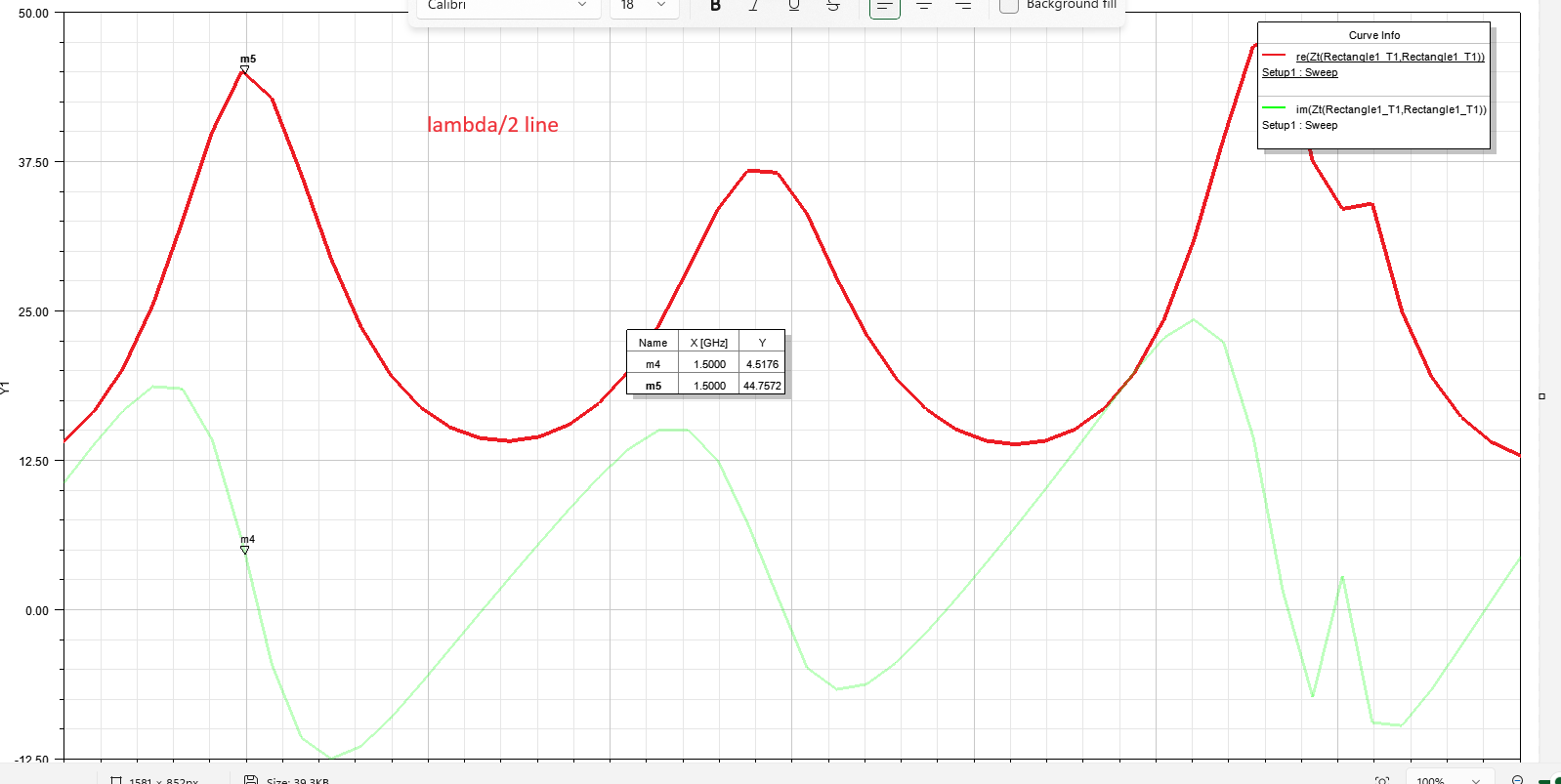
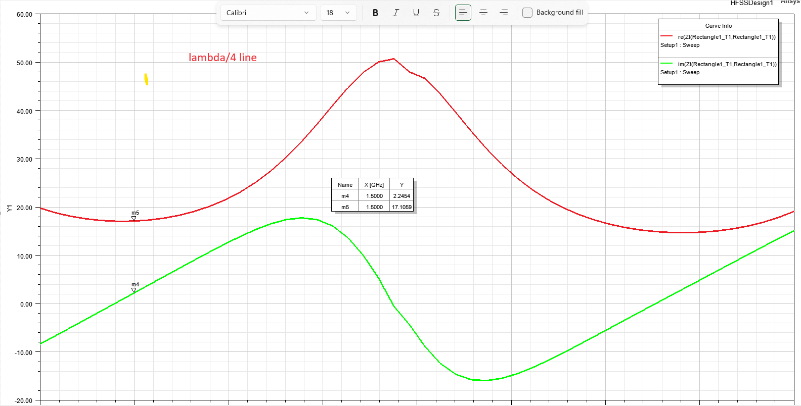
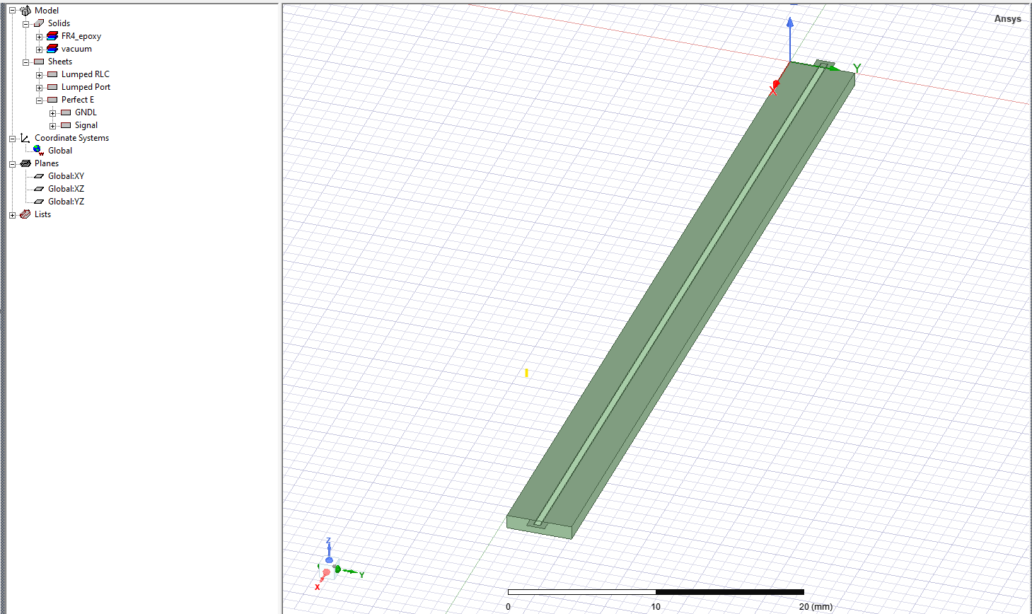
I am designing single port (50 ohms) coplanar waveguide of 50 ohms in HFSS which is connected to other end with 50 ohm lumped RLC component. The width and spacing of the waveguide is 0.412733mm and 0.05mm respectively in FR4_epoxy substrate (er=4.4). Since characteristic impedance of CPW is Zo= 50 ohm which is connected to load of ZA=50 ohm, using the following below relation, Zin should be always 50 ohms irrespective of βL based on mathematics as numerator and denominator being same. Thus, it should be same for all frequencies and all βL. I tried for lambda/2 and lambda/4 length (calculated using ADS linecalc for 1.5GHz) for 1 to 5GHz but could not achieve the constant 50 ohm input impedance for all frequencies or at 1.5GHz for two different length. I highly appreciate the help on this how to achieve my requirement. The design and simulation result are attached below.

1698448866851.png


1698449470440.png
1698450241369.png

1698450338729.png
 
Hello Tony,

Thank you for the reply. Actually, I am trying to simulate for CPW transmission line instead of grounded CPW for my work. I have attached the screenshot of calculation for CPW here as I am limited to use 0.05mm gap between the signal and ground pour. Based on mathematics if characteristic impedance is equal to load impedance then Zin should be equal to Z0 for all frequencies or Zin is not dependent to transmission line length. I also understand that it might be little different in the simulation platform than theory. However, I am assuming the Zin should be around 50 ohm for all frequencies for simulation as well which I am not getting. Thank you again for your help.

1698476690953.png
 
According to impedance curve, we see TL Z0 of about 29 ohm, terminated with 50 ohm.
Thank you for the reply. The transmission line is designed for 50 ohm. Please find the attached screenshot. However, I am not getting the constant 50 ohm impedance for overall frequency.

1698476772921.png
 
I wonder if you have used exactly the same geometry in HFSS and in Linecalc? Linecalc shows rather unphysical conductor height of 0.15 um. If you had e.g. used 0.15 mm in HFSS, the impedance value would be plausible. This can be only checked in HFSS model.

I would also comment that 0,05 mm ground separation can't be manufactured in most PCB technologies, and if you have an advanced technologie supporting this structure width, it won't be very accurate.

Post #2 suggests Saturn PCB toolkit, but it doesn't support CPW without ground or different counductor height for CPW.
 
1) Please show a zoomed in view of your port configuration.

port.jpg


2) Your approach to use a lumped termination instead of port 2 is unusual. You should figure how how to get Zin (not Z11!) from 2-port simulation in HFSS. Many EM solvers have such Zin parameter readily available, otherwise you can calculate it from S11.

3) Have you included metal thickness in simulation? It will be relevant at this extremely narrow gap. Also, in real world the solder mask will have a strong effect at this narrow gap width, not to mention FR4 fibre pattern ...
 
I wonder if you have used exactly the same geometry in HFSS and in Linecalc? Linecalc shows rather unphysical conductor height of 0.15 um. If you had e.g. used 0.15 mm in HFSS, the impedance value would be plausible. This can be only checked in HFSS model.

I would also comment that 0,05 mm ground separation can't be manufactured in most PCB technologies, and if you have an advanced technologie supporting this structure width, it won't be very accurate.

Post #2 suggests Saturn PCB toolkit, but it doesn't support CPW without ground or different counductor height for CPW.
Yes, I am using exact same width and spacing in HFSS like ADS. Screenshot attached; In HFSS for now to make it more simpler I am using rectangular sheet (0 thickness and perfect conductor). Do you think this is making difference? Yes, I understand 0.05mm spacing is not possible in PCB technologies. Actually, I am using other substrate for which 0.05mm is possible but to make myself clear in concepts, I am using FR4 substrate before diving into actual substrate. Also, I am limited to CPW not in Grounded CPW. Thank you again for your help.

1698509359308.png
 
1) Please show a zoomed in view of your port configuration.

View attachment 185811

2) Your approach to use a lumped termination instead of port 2 is unusual. You should figure how how to get Zin (not Z11!) from 2-port simulation in HFSS. Many EM solvers have such Zin parameter readily available, otherwise you can calculate it from S11.

3) Have you included metal thickness in simulation? It will be relevant at this extremely narrow gap. Also, in real world the solder mask will have a strong effect at this narrow gap width, not to mention FR4 fibre pattern ...
Please find the attached screenshot for the zoomed version of port which is similar in other end with lumped RLC element. I did two port simulation as well and calculated input impedance using relation
zin=z11-(z12*z21)/(z22+zl); where Zl=50 ohms from second port. However, it is also not giving 50 ohm. No, to make it simpler I chose rectangular sheet (0 thickness and perfect conductor). Does this make this much difference? For real world I am using different substrate and I will not have the problem of solder mask there but I wanted to make my concept clear using FR4 which is widely used substrate and dive to the actual substrate that I need. Thank you again for your help.

1698509860753.png
 
Please find the attached screenshot for the zoomed version of port which is similar in other end with lumped RLC element.
It is difficult to understand what we see here. You have some length standing out at the end, extending over the PCB substrate material?

What port type did you use? I don't see any port in your screenshot. A short lumped port length would mean large parasitic C from signal to ground conductor across the port, and HFSS has no port calibration to remove that effect.
 
I'm not sure how your ports are setup, but I would recommend not using what you've shown at this stage.

Validate your results using a waveport first; then proceed to more realistic lumped port simulations.
 
It is difficult to understand what we see here. You have some length standing out at the end, extending over the PCB substrate material?

What port type did you use? I don't see any port in your screenshot. A short lumped port length would mean large parasitic C from signal to ground conductor across the port, and HFSS has no port calibration to remove that effect.
Yeah that was connecting two grounding plane together and assigning lumped port in between. However, I changed the structure and put it inside. I have attached screenshot of whole design and port connection here. The port used is lumped port. The length and width of the port are equal to width of the signal trace which is in between the signal trace and two merged ground.
1698722943941.png
1698722987773.png


The length and width of signal trace and the spacing between signal trace and ground pour is obtained from the circuit of HFSS for 6GHz for lamda/2. Please find the attached screenshot which gives 50+i*50 at 6 GHz since zin=Zl and Zl+50+i*50. However, when I used all the values same in HFSS model it is not same. Though HFSS model does not directly support Zin calculation, I defined output variables using Zin=Z11-(Z12*Z21)/(Z22+ZL) and plotted. The screenshot is below. I understand there might be some loss in HFSS model not ideal like circuit model but it is off quite a bit. How can I minimize the loss and get Zin=Zl when using lambda/2 line.

This is result from circuit modelling of Ansys.
1698723424048.png
1698723454894.png


This is result from HFSS modelling.

1698723587032.png
1698723625764.png


Any help will be highly appreciated.
 
I designed 50 ohms lambda/2 microstrip line and wanted to verify if it is exactly lambda/2 and 50 ohms line or find what losses might be there by looking into complex load impedance since the Zin should equals to ZL if it is lambda/2 line. However, when I did it in circuit simulation it is giving me decent result but when used same parameters (length=15.2212 mm, width=0.411079 and spacing =0.05mm) in HFSS design the real impedance is off a lot though complex impedance is close.
 
You are using many strange test methods. :unsure:
Why don't you look at S-parameters to verify that S21 phase is 180°?

But anyway, I built my own 3D EM model using your dimensions, using Empire XPU (FDTD) solver. I used a wave port (QTEM port) and get very good matching, return loss is better than 30dB. Metal is zero thickness, as you modelled in linecalc. Screenshots below!

So the issue is your HFSS model. I would recommend that you look at post #11: using wave ports will avoid possible error sources from port parasitics. But there are many other possible mistakes in using EM solvers, so take your time to learn using the tool!

cpw1.png


cpw2.png
 
Thank you so much for the guidance and observing phase S21 to verify if designed transmission line is lambda/2 is a great idea. I designed the wave port accordingly. The S21 phase is around 178 degree and input impedance seems to be little off which I believe is related to thickness of PEC backing needed in wave port since changing the thickness is taking me closer to 50 ohms and 180 degrees. When I change the port impedance to 70 ohms the input impedance is 66ohms which is quite a bit off. I checked HFSS manual and there is no any explanation related to thickness of PEC backing. Could you please help me what should be the thickness of PEC backing or if it is related to something else? I am looking for exact ZL impedance in input impedance at least in simulating platform like circuit simulator since after this I am designing a matching network for different load using transformer and so on and input impedance having little off also change a lot. I highly appreciate your help on this.
--- Updated ---

You are using many strange test methods. :unsure:
Why don't you look at S-parameters to verify that S21 phase is 180°?

But anyway, I built my own 3D EM model using your dimensions, using Empire XPU (FDTD) solver. I used a wave port (QTEM port) and get very good matching, return loss is better than 30dB. Metal is zero thickness, as you modelled in linecalc. Screenshots below!

So the issue is your HFSS model. I would recommend that you look at post #11: using wave ports will avoid possible error sources from port parasitics. But there are many other possible mistakes in using EM solvers, so take your time to learn using the tool!

View attachment 185891

View attachment 185892
Thank you so much for the guidance and observing phase S21 to verify if designed transmission line is lambda/2 is a great idea. I designed the wave port accordingly. The S21 phase is around 178 degree and input impedance seems to be little off which I believe is related to thickness of PEC backing needed in wave port since changing the thickness is taking me closer to 50 ohms and 180 degrees. When I change the port impedance to 70 ohms the input impedance is 66ohms which is quite a bit off. I checked HFSS manual and there is no any explanation related to thickness of PEC backing. Could you please help me what should be the thickness of PEC backing or if it is related to something else? I am looking for exact ZL impedance in input impedance at least in simulating platform like circuit simulator since after this I am designing a matching network for different load using transformer and so on and input impedance having little off also change a lot. I highly appreciate your help on this.
 
When I change the port impedance to 70 ohms the input impedance is 66ohms which is quite a bit off.
Simulated line impedance should not depend on port impedance!

Not sure why you get 66 Ohm. My line impedance result for your dimensions is around 45 Ohm, for pure CPW on the top layer with not metal on PCB Bottom layer.

I cannot help you with HFSS port setup, but others who are more familiar with HFSS might jump in. And of course, there are dozens of settings in HFSS which have an influence on accuracy. Why don't you post your HFSS model, so that other users can check what your mistake is?

Hello there,

I have attached my design files here with both circuit model and HFSS model. Load impedance is set as 70+50i and expecting input impedance same which I obtained in cicruit model. I am designing lambda/2 line with 50 ohms impedance and waveports are used. Input impedance in HFSS is calculated as ouptut variables using Zin=Zo*(1+S11)/(1-S11).

Any help will be highly appreciated.
 

Attachments

  • CPW.zip
    79.4 KB · Views: 43

LaTeX Commands Quick-Menu:

Similar threads

Part and Inventory Search

Welcome to EDABoard.com

Sponsor

Back
Top