Continue to Site
Follow along with the video below to see how to install our site as a web app on your home screen.
Note: This feature may not be available in some browsers.

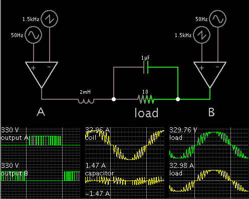
It should be okay for you to make the connections you describe. It can work because the transformer secondaries themselves are not connected to each other.
after few seconds a sound came

is it possible to show me the DC-link current?


@BradtheRad: Thanks for your valuable feedback.I tried to make circuit in Circuit Simulator v1.6i to check the waveform as you gave in the above post but didn't find the Triangular wave generator

