Continue to Site

Welcome to EDAboard.com

Welcome to our site! EDAboard.com is an international Electronics Discussion Forum focused on EDA software, circuits, schematics, books, theory, papers, asic, pld, 8051, DSP, Network, RF, Analog Design, PCB, Service Manuals... and a whole lot more! To participate you need to register. Registration is free. Click here to register now.

Common Source Single stage amplifier with PMOS diode connected Load

Status
Not open for further replies.

20tech11

Junior Member level 3
Joined
Oct 23, 2010
Messages
26
Helped
3
Reputation
6
Reaction score
3
Trophy points
1,283
Location
Edinburgh, Scotland
Activity points
1,444
Hi all,

Can any one tell me how the DC response of the PMOS diode connected load of NMOS driver, gives VDD- VTH if we neglect the Subthreshold currrent and More than VDD- VTH if we consider the subthreshold current?

My doubt is like when the input voltage is 0, the NMOS is OFF, but a output voltage is VDD- VTH !!! How should it be? As there is no current flow, how the vout can be VDD- VTH?

Please tell me the effect of subthreshold current too!!!

Thanks
Vineeth
 

My doubt is like when the input voltage is 0, the NMOS is OFF, but a output voltage is VDD- VTH !!! How should it be? As there is no current flow, how the vout can be VDD- VTH?
"(Absolutely) no current flow" doesn't exist in reality. The voltage at the connection node is still VDD-VTH, even if the current is in the fA range (1e-15 A ≈ 6000 electrons/s), because the pmos diode's impedance « impedance of the switched-off nmos.

Please tell me the effect of subthreshold current too!!!
Read books on analog design, e.g.
[Allen/Holberg] "CMOS Analog Circuit Design"
David M. [Binkley] "Tradeoffs and Optimization in Analog CMOS Design"
Behad [Razavi] "Design of Analog CMOS Integrated Circuits"
 

Hi Erikl,

Thank you very much..
1. But I can't understand how it can be VDD-VTH. If it is VDD-VTH, th PMOS is ON and the full inversion layer should have been formed. In Diode connected amplifier, how the GATE( Drain voltage of both NMOS and PMOS)voltage of PMOS reaches to VTH with 0 input voltage? I am really confused to explain the working of the circuit when 0 <= Vin < VTH. Could you pleae help in this?

2. But even if current is in fA range and the drop across PMOS should be less than VDD-VTH! Am I correct?

3. Also I can't understand why the PMOS' output impedence is less than the NMOS? I have taken measurements with PMOS and NMOS and I have got almost same result..I have got 98 K for PMOS measures between VDS (-4.5V and - 3.5V) and for NMOS 188.5 K measured between VDS ( 4.99 V and 4.5 V) with VDD = 5V. Could you please clear my dobts?

Thanks for your help!!!
Vineeth


"(Absolutely) no current flow" doesn't exist in reality. The voltage at the connection node is still VDD-VTH, even if the current is in the fA range (1e-15 A ≈ 6000 electrons/s), because the pmos diode's impedance « impedance of the switched-off nmos.


Read books on analog design, e.g.
[Allen/Holberg] "CMOS Analog Circuit Design"
David M. [Binkley] "Tradeoffs and Optimization in Analog CMOS Design"
Behad [Razavi] "Design of Analog CMOS Integrated Circuits"
 

1. But I can't understand how it can be VDD-VTH. If it is VDD-VTH, th PMOS is ON and the full inversion layer should have been formed. In Diode connected amplifier, how the GATE( Drain voltage of both NMOS and PMOS)voltage of PMOS reaches to VTH with 0 input voltage? I am really confused to explain the working of the circuit when 0 <= Vin < VTH. Could you pleae help in this?
If I understand you correctly, you want to study the situation for Vin=0 (Vgs(nmos)=0). In this case, there's only leakage current through both fets. The diode-connected pmos, however, will not have (Vgs(pmos)=0), because its gate is connected to its drain, hence 0 ≤ Vgs(pmos) ≤ VTH(pmos).

2. But even if current is in fA range and the drop across PMOS should be less than VDD-VTH!
VDD-VTH is not the drop across PMOS, but the voltage at the common node referred to GND.

3. Also I can't understand why the PMOS' output impedence is less than the NMOS?
The reason is: |Vgs(pmos)| > Vgs(nmos)=0
 

Hi ,

2. But I am confused how the output node has voltage generated when Vin = 0..Is it because of the subthreshold current??

Vineeth.

If I understand you correctly, you want to study the situation for Vin=0 (Vgs(nmos)=0). In this case, there's only leakage current through both fets. The diode-connected pmos, however, will not have (Vgs(pmos)=0), because its gate is connected to its drain, hence 0 ≤ Vgs(pmos) ≤ VTH(pmos).


VDD-VTH is not the drop across PMOS, but the voltage at the common node referred to GND.


The reason is: |Vgs(pmos)| > Vgs(nmos)=0
 

I am confused how the output node has voltage generated when Vin = 0..Is it because of the subthreshold current??
Yes. Usually called leakage current for Vgs=0, and subthreshold current for 0 ≤ Vgs ≤ VTH.
 
So I have a question about this topology. In Razavi's text Design of Analog CMOS ICs he proves that gain is proportional to the ratio of the overdrive voltage of the pmos to the nmos.

Av = |Vgs2 - Vth2| / |Vgs1 - Vth1|

But then he says gain is ~ gm1/gm2 which means gain is inversely proportional to the above. He acknowledges the paradox but I don't know why this occurs or what it implies?

Any thoughts?
 

Av = |Vgs2 - Vth2| / |Vgs1 - Vth1|
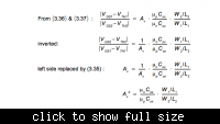
Above equation (Razavi's (3.35) in my edition) implies correctly adapted W/L ratios of both transistors and their µn/µp ratio as well, whereas Av=gm1/gm2 (3.36) resp. (3.37) still contains these ratios. I think Razavi's Example 3.3 and its solution (on the same page, below) explains this quite well.

And here comes the math:
 

I understand your math but can you explain why (3.35) shows Av = |Vgs2 - Vth2| / |Vgs1 - Vth1| while Av ~ |Vgs1 - Vth1| / |Vgs2 - Vth2| from (3.36) and (3.37). This is like saying A=1/A.
 

If you retrace my math thouroughly you should understand that the two equations are consistent: Draw the root on the last equation shown above and get Razavi's equation (3.33) :

\[ A_v ~ = ~ - \sqrt {{{\mu_n C_{ox}} \over {\mu_p C_{ox}}} ~ \cdot ~ {(W/L)_1 \over (W/L)_2}} \]
 

Status
Not open for further replies.

Similar threads

Part and Inventory Search

Welcome to EDABoard.com

Sponsor

Back
Top