Continue to Site

Welcome to EDAboard.com

Welcome to our site! EDAboard.com is an international Electronics Discussion Forum focused on EDA software, circuits, schematics, books, theory, papers, asic, pld, 8051, DSP, Network, RF, Analog Design, PCB, Service Manuals... and a whole lot more! To participate you need to register. Registration is free. Click here to register now.

CMFB for a 2 stage opamp (continuous)

Status
Not open for further replies.

mretsh91

Junior Member level 3
Joined
Jan 26, 2013
Messages
28
Helped
1
Reputation
2
Reaction score
1
Trophy points
1,283
Visit site
Activity points
1,509
I am working on a 2 stage fully differential op amp, but I have a problem with the CMFB ...please I need help with the suitable CMFB ??? I believe that I need only 1 cmfb block that will adjust both stages ,,,but I don't know the suitable technique ...I want to apply it now only using ideal vcvs and sensing using resistors ...just behavioral
thanks in advance
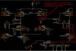
2stage_opamp.png
 

Sense the output vo_l_2 and vo_r_2 using using resistive divider. Give the output of the resistive divider to one input of a transconductor (vccs). Connect common mode reference voltage vcm to the other input. Connect the output of vccs to cmfb1. Ensure the polarity of transconductor such that when vo_l_2 and vo_r_2 tend to increase, cmfb1 tend to decrease. You may also have to compensate for the cmfb loop.
 
First of all, I'd like to thank u monsoon for ur concern.
Now I implemented the configuration in your comment, the output of the second stage is fixed correctly at 0.6v (I am using 1.2V supply) but the first stage was not fixed ......why does this happen ...although I understand that this point must be Vdd/2 to let the current in the upper Mos to be equal to the current in the lower one.
q1.png
 

but the first stage was not fixed ......why does this happen
By nature of a two-stage amplifier. It's neither feasible nor useful to bias the first stage output to Vdd/2. The bias point of the first stage is commanded by Vth of the second stage transistors.
 
Output of the first stage will not be fixed to 0.6. First stage output is determined by the Vsg of the PMOS transistors M8 and M9. In other words, common mode feedback will ensure that the output of the first stage is such that current through M9 (M8) is exactly equal to current through M16 (M18). You can adjust the first stage voltage by changing the W/L ratio of M8 and M9.
 
By nature of a two-stage amplifier. It's neither feasible nor useful to bias the first stage output to Vdd/2. The bias point of the first stage is commanded by Vth of the second stage transistors.

Could u please explain more why it is not feasible, as by equations:
For PMOS to be in SAT

Vsd>Vsg-Vth
-Vd > -Vg- Vth
Vd< Vg+Vth
if Vd=0.6, by CMFB at secong stage
Vg>Vd-Vth
-->Vg>0.6-Vth Then according to this point (Vg) can reach Vdd/2.

why it is not feasible then ????
thanks again

- - - Updated - - -

Thanks alot monsoon...ur comments were very helpful to me .... I got ur point :)
I have one more question please, do I have to adjust the W/L ratios at the first stage to maintain the middle node (Vo_r) at 0.6 or it is useless.
Thanks again

- - - Updated - - -

Output of the first stage will not be fixed to 0.6. First stage output is determined by the Vsg of the PMOS transistors M8 and M9. In other words, common mode feedback will ensure that the output of the first stage is such that current through M9 (M8) is exactly equal to current through M16 (M18). You can adjust the first stage voltage by changing the W/L ratio of M8 and M9.


Thanks alot monsoon...ur comments were very helpful to me .... I got ur point :)
I have one more question please, do I have to adjust the W/L ratios at the first stage to maintain the middle node (Vo_r) at 0.6 or it is useless.
Thanks again
 

You'll have to adjust the bias current either of first or second stage to get 0.6V bias at the first stage output. But what is it good for?
 
You'll have to adjust the bias current either of first or second stage to get 0.6V bias at the first stage output. But what is it good for?

As I understand, I think it has no point to adjust the first stage to 0.6 as the loop will ensure the current equality in the first stage mirrors
 

I have one more question please, do I have to adjust the W/L ratios at the first stage to maintain the middle node (Vo_r) at 0.6 or it is useless.
Swing at the first stage is very small. So biasing the common mode of the first stage to 0.6V is not necessary.
 
Please I have one more question concerning this opamp, I will use it as an integrator in a system with a sampling frequency of 384MHZ, so I want my opamp GBW to be about 1GHZ .... I want to know which loop shall be my GBW and determine my PM:

1-Breaking up the CMFB lope using CMDM probe
2-Breaking up the integrator loop

or what else ?????
Selection_002.png

Actually, I am used to single ended opamp where I perform my design on the open loop as I don't have to implement CMFB ,, but at the fully differential case I am a little bit confused.

Thanks in advance
 

Now I have my CMFB bode plots are totally unstable although the output is adjusted to 0.6v .....please help
cmfb_loop.png
 

This CMFB loop has 3 stages which tend to make it unstable. Keep reducing the the transconductance of vccs used. Also reduce the value of common mode sensing resistors. Try using a compensating caps between cmfb1 and vo_l, cmfb1 and vo_r.
 
The low frequency loop gain phase isn't plausible. Looks like an erroneous "measurement" at first sight. Appart from this point, a gain of 10e5 for the CFMB error amp seems completely unrealistic.
 
. Appart from this point, a gain of 10e5 for the CFMB error amp seems completely unrealistic.

Please note that I changed the value in the upper circuit (0e5 ) to 40 while doing these plots only, and thanks for your note :)
but I have a question please, Isn't this gain represents both the CMFB gain and the OP-Amp gain ??

- - - Updated - - -

This CMFB loop has 3 stages which tend to make it unstable. Keep reducing the the transconductance of vccs used. Also reduce the value of common mode sensing resistors. Try using a compensating caps between cmfb1 and vo_l, cmfb1 and vo_r.

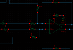
I have reduced my transconductance to 40 now, but I noticed that once I connect the load resistance -as shown in the attached image- the system is totally unstable
cct2.png
 
Last edited:

The low frequency loop gain phase isn't plausible. Looks like an erroneous "measurement" at first sight.error amp seems completely unrealistic.

Yes, we noticed that it is weird , but i believe it means it is totally unstable ... we assumed that's what it means because we don't think there are any errors in the connections or the stability analysis configuration.

Thanks for your concern.
 

First of all, I'd like to thank you both monsoon and FvM for your help. Actually you were very helpful to me and I really appreciate it.
Second, I am going to re-deign my op-amp again after I understood some fundamental points. So, I just want you guys to explain the relation between both loops (the differential loop and the CMFB loop) while design as I find it difficult to achieve both loops system requirements.
Thanks in advance guys
 

Status
Not open for further replies.

Part and Inventory Search

Welcome to EDABoard.com

Sponsor

Back
Top