Continue to Site

Welcome to EDAboard.com

Welcome to our site! EDAboard.com is an international Electronics Discussion Forum focused on EDA software, circuits, schematics, books, theory, papers, asic, pld, 8051, DSP, Network, RF, Analog Design, PCB, Service Manuals... and a whole lot more! To participate you need to register. Registration is free. Click here to register now.

Clapp oscillator signal distortion.

Status
Not open for further replies.

stambaughw

Junior Member level 1
Joined
Feb 26, 2014
Messages
17
Helped
0
Reputation
0
Reaction score
0
Trophy points
1
Activity points
189
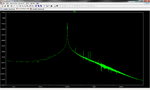
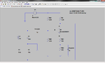
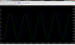
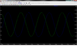
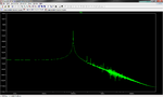
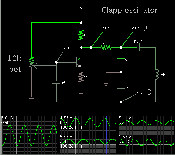
I'm trying to simulate a ~100KHz clapp (or culpitt) oscillator circuit (see clapp-osc-schematic.png) using LTSpice and I'm getting an odd distortion in the output which I cannot figure out how to eliminate. I noticed the the current through Cbypass (see clapp-osc-waveforms.png) seems to be where things are falling apart but I'm not sure what is causing this distortion. By lowering Cbypass I can decrease the distortion to a point (but not completely eliminate) but but if I go too low the oscillation is dampened out. I would prefer that the output not have this distortion before I attempt to bread board this circuit. As you can see from the FFT (see clapp-osc-fft.png) analysis, there are quite a few less than desirable harmonics in the signal. I'm stumped as to how to eliminate this distortion so any help would be greatly appreciated. For some reason the thread editor would not let me attach the LTSpice and transistor model files but I can email them if that is helpful.
 

Attachments

  • clapp-osc-fft.png
    clapp-osc-fft.png
    62 KB · Views: 109
  • clapp-osc-schematic.png
    clapp-osc-schematic.png
    65.1 KB · Views: 129
  • clapp-osc-waveforms.png
    clapp-osc-waveforms.png
    73.2 KB · Views: 101

It is the purpose of the bypass capacitor (normally) to short the ac signal.
In your case, it has a rather small value (1nF) and, hence, partly determines the gain of the transistor stage (and causes phase distortions).
My recommendation: Increase the bypass capacitor to a large value (100 nF).
As a consequence, the gain of the stage could be too large (signal clipping).
Therefore, decrease the gain by adjusting the resistors only (RC and/or RE1)
 
I lowered RC and raised RE1 as shown. I also had to lower RE2 to keep the collector voltage from getting to high. With the 350 ohm resistor in RE2 my output was getting too close to the 5V rail for my comfort. I still could not get rid of all of the distortion. There is still some minor distortion on the lower half of the current through Cbypass which is difficult to see in the waveform plot. If I lower the gain any further, the oscillations start to dampen out and if I raise the gain the distortion gets worse. I'm a bit concerned that I may be operating too close to the margins for reliable operation. Am I expecting too much from this circuit? Are there additional measures I can take to improve the performance of this circuit?

- - - Updated - - -

Just so I'm clear, you mean replace resistor RC with a LC tank circuit and get rid of the tapped capacitor arrangement in the feedback path? Is feedback path between the collector and the Ccouple still required in this configuration?
 

Attachments

  • clapp-osc-schematic2.png
    clapp-osc-schematic2.png
    67.7 KB · Views: 86
  • clapp-osc-waveforms2.png
    clapp-osc-waveforms2.png
    68.2 KB · Views: 78
  • clapp-osc-fft2.png
    clapp-osc-fft2.png
    61.2 KB · Views: 84
Last edited:

stambaugh, what do you expect from the circuit?
For my opinion, the signal looks good and the distortios have disappeared, are they not?

It is quite normal that you - more or less - are "balancing on a rasors edge".
That`s a normal behaviour for oscillators without an additional amplitude control mechanism:
* Loop gain slightly smaller than unity: oscillations dampen out.
* Loop gain slightly larger than unity: rising amplitudes with clipping.
 
If RC is a resonant parallel LC then it passes the wanted frequency and attenuates unwanted frequencies.
Of course the tapped capacitors are needed to provide the proper phase shift for positive feedback and for oscillation to occur.

The circuit designed "on a razor's edge" might not work if the transistor is at one end of its spec's.
 

That`s a normal behaviour for oscillators without an additional amplitude control mechanism:
* Loop gain slightly smaller than unity: oscillations dampen out.
* Loop gain slightly larger than unity: rising amplitudes with clipping.

That's the key.
You will always have some distortion (because of clipping) for stable oscillation in this type of circuit.
You can get less distortion reducing the loop gain of the stage, but if you go near the limit you risk that it fails to maintain oscillation if something changes (temperature, supply voltage, or if you replace the transistor by another one of the same type but slightly different).
The signal can be further filtered if you need less harmonic distortion.
Regards

Z
 
Why do you need the bypass cap at all? Normally, the purpose of such a capacitor is only to increase signal gain (by lowering the signal feedback).
But that is not the case in this application. In contrary - signal feedback caused by an emitter resistor has advantages.
 
That's the key.
You will always have some distortion (because of clipping) for stable oscillation in this type of circuit.
You can get less distortion reducing the loop gain of the stage, but if you go near the limit you risk that it fails to maintain oscillation if something changes (temperature, supply voltage, or if you replace the transistor by another one of the same type but slightly different).
The signal can be further filtered if you need less harmonic distortion.
Regards

Z
I will have to error on the side of too much gain because this circuit has to work over temperature and tolerate the differences in transistor operating specs. Operating on the razors edge is always dangerous. I like to avoid it whenever I can.
 

There are several places where you might tap for your output.

Here is a simulation showing waveforms at several nodes.

I located the LCC tank at the right, because the greatest current flow takes place there, and because it is the load (in a manner of speaking).

I omitted the RC network in the emitter leg.


My schematic might still need further adjusting to reduce distortion.

I'm not saying it will necessarily suit your real-life purposes better than your own schematic.
 
. Operating on the razors edge is always dangerous. I like to avoid it whenever I can.

* For any oscillator - this can be avoided only using a non-linear element that automatically adusts the gain for rising amplitudes (diodes, FET control loop,...)
That is the normal way to design a low THD oscillation signal.

* As an alternative, you can allow some sort of clipping if you have the chance to pick up the signal after some kind of bandpass filtering (see the contribution from BradTherad) ); as an alternative you can use an additional extern bandpass for filtering purposes.
 

There are several places where you might tap for your output.

Here is a simulation showing waveforms at several nodes.

I located the LCC tank at the right, because the greatest current flow takes place there, and because it is the load (in a manner of speaking).

I omitted the RC network in the emitter leg.


My schematic might still need further adjusting to reduce distortion.

I'm not saying it will necessarily suit your real-life purposes better than your own schematic.

I'm assuming the 220 ohm resistor is to prevent the collector of the transistor from seeing an AC short across the output capacitor (5.6nF) that is tied to the supply return.
 

* For any oscillator - this can be avoided only using a non-linear element that automatically adusts the gain for rising amplitudes (diodes, FET control loop,...)
That is the normal way to design a low THD oscillation signal.

Would the non-linear element need to be in the feedback path and if so where? If it all it would take is a diode to clean up this distortion, that would be ideal.
 

I am afraid - in your case, it is not such easy. In general, a soft amplitude control is relatively simple if the oscillator can be split in two different parts:
*Finite gain amplifier (symmetrical to ground potential)
* and the frequency-determining passive network.

Typical examples for this class of oscillators are opamp-based oscillators.
For transistor oscillators, the situation is somewhat more complicated because the ouput signal is not symmetrical to ground potential.
In this case, a control loop is to be created in order to reduce the gain for rising ampitudes.

As an example, the following link describes a control loop (using another transistor) which reduces the quiescent collector current (therby reducing the gain).

https://litetec.hubpages.com/hub/An-Amplitude-Stabilized-Oscillator-Circuit
 

Isn't the internet FULL of mistakes? The "Complementary Feedback Pair" is WRONG and Sziklai will be insulted:
 

Attachments

  • Sziklai pair.png
    Sziklai pair.png
    113.4 KB · Views: 75

Isn't the internet FULL of mistakes?

Yes - tat´s true. In general, I never would blindly trust such information.
However, as we know, the same applies also to other (printed) knowledge sources - in particular nowadays when it is so simple to create some printed pages (in form of text books).
 

I also made a mistake with my "correction". The resistors should not have the same value unless the supply voltage is very low.
I corrected it again here:
 

Attachments

  • Sziklai pair.png
    Sziklai pair.png
    122.4 KB · Views: 70
What you are seeing on spectrum analyzer are harmonics of fundamental 100kHz signal. Harmonics are more than 40dB lower than fundamental signal what means that THD is about 1%. Result seems to be OK. Lowpass filter on output signal will lower the harmonics more than linearisation of amplifier.
 
  • Like
Reactions: FvM

    FvM

    Points: 2
    Helpful Answer Positive Rating
Besides the said faults, I won't consider the posted two transistor circuit as amplitude control loop example, because it misses a rectifier and averaging filter. It's just another case of more or less soft clipping, with respective harmonic distortions.

I'd also emphasize that -40 dBc distortion isn't bad for a LC oscillator without gain control.
 

I'm assuming the 220 ohm resistor is to prevent the collector of the transistor from seeing an AC short across the output capacitor (5.6nF) that is tied to the supply return.

I guess you could say that. Another purpose is to adjust current kicks which are applied to the LC tank. A few mA kick is all it takes, to sustain oscillations in the LC tank.

The three resistors reduce current in the circuit to a low level.

Both collector resistors are needed.

The emitter resistor reduces gain, in addition to causing less drastic gain swings when adjusting bias.
 

Status
Not open for further replies.

Similar threads

Part and Inventory Search

Welcome to EDABoard.com

Sponsor

Back
Top