Smillsey
Member level 5
Hi all!
I have a deisgn in which i have multiple signals entering a DG1208 mux.
I am using ada4807 op amps both before (to provide gain) and after (as a buffer) the DG1208.
At the output of the DG1208 pin 8 (COM) is a non-inverting buffer as follows;

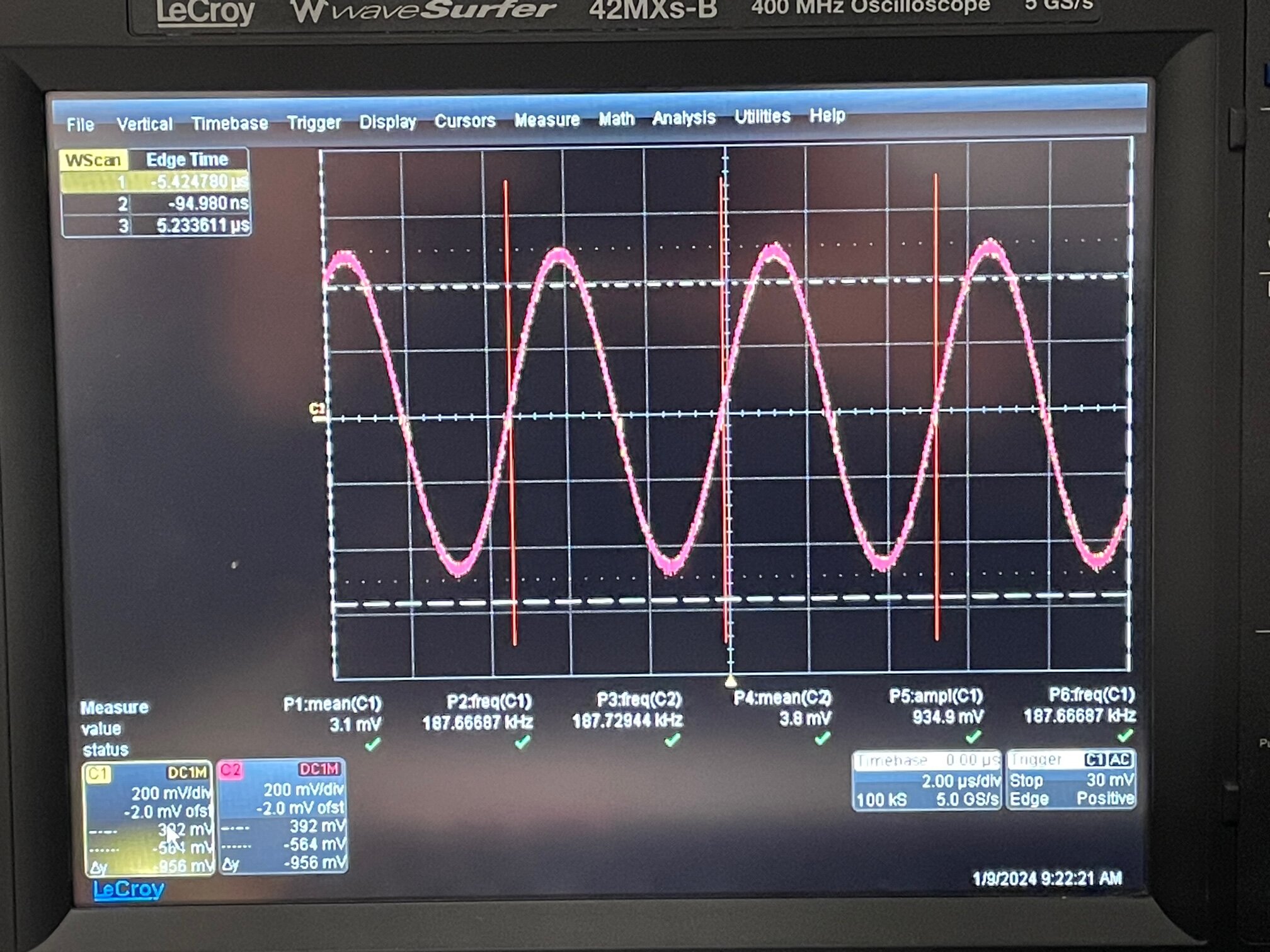
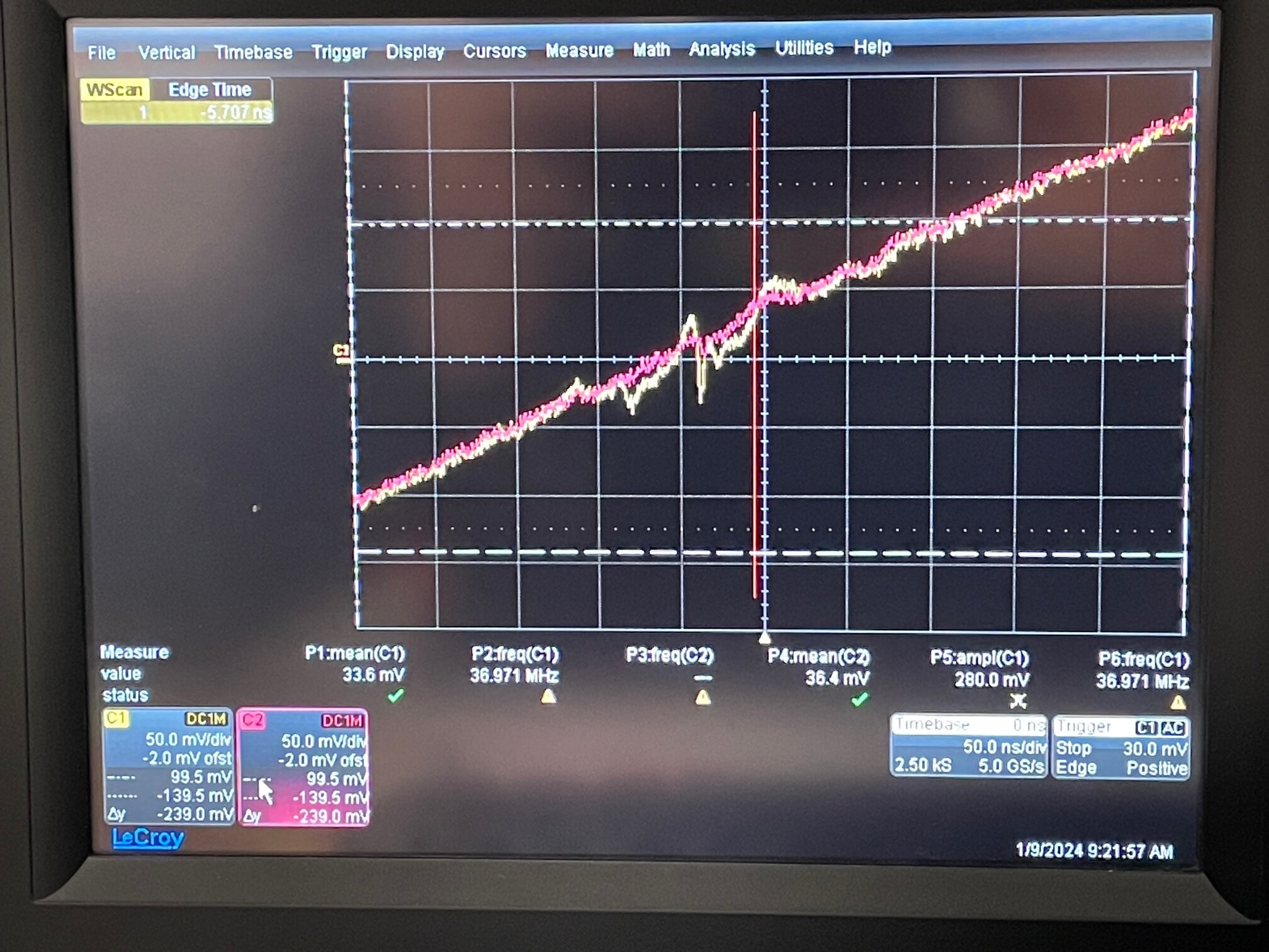
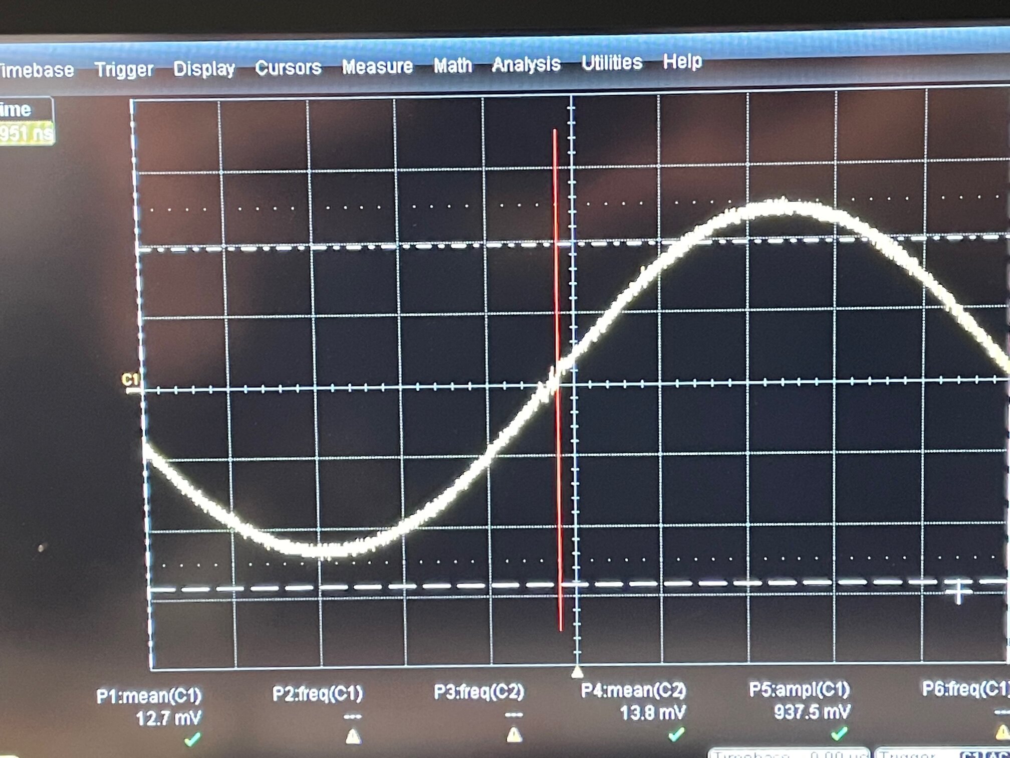
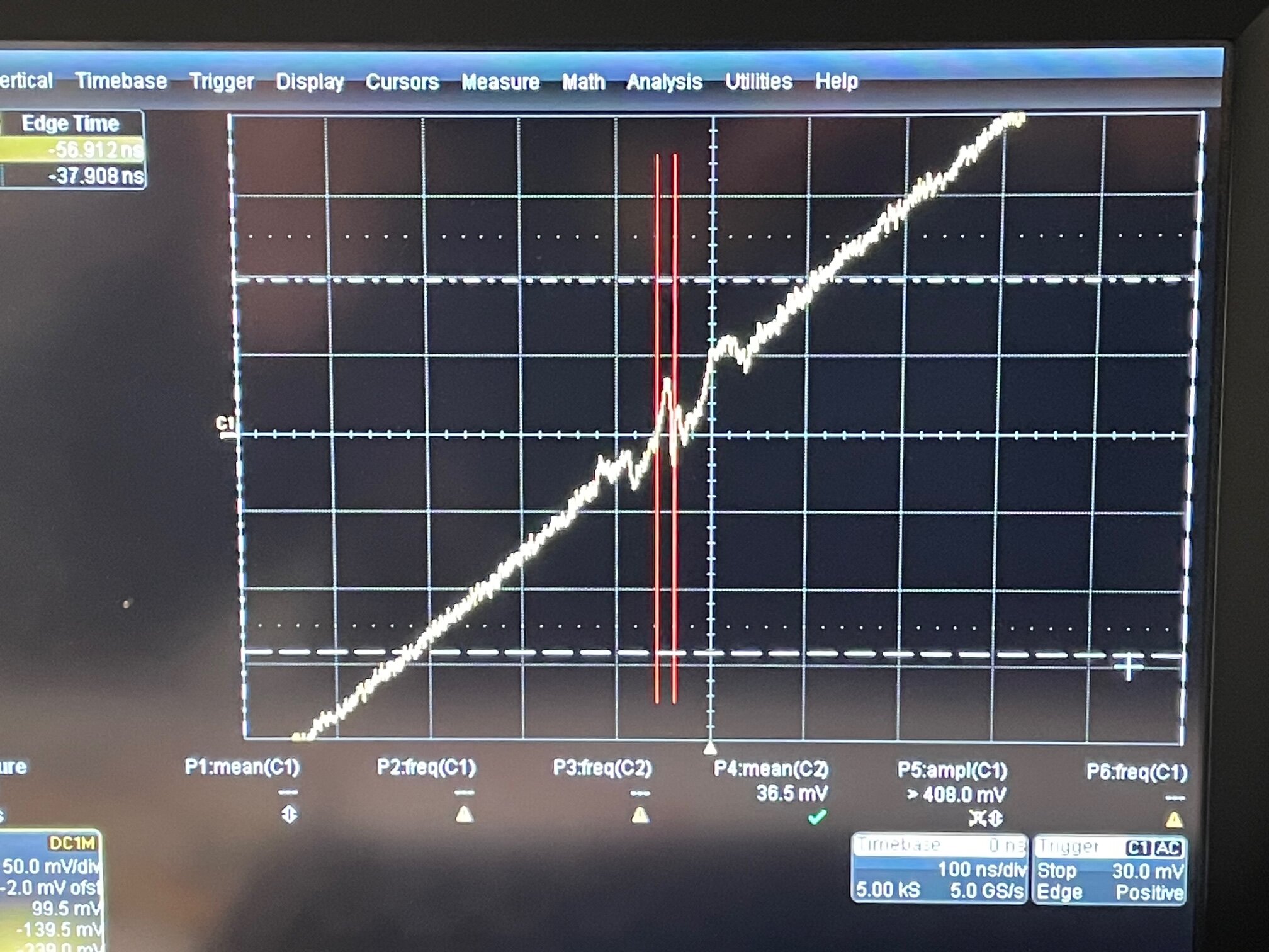
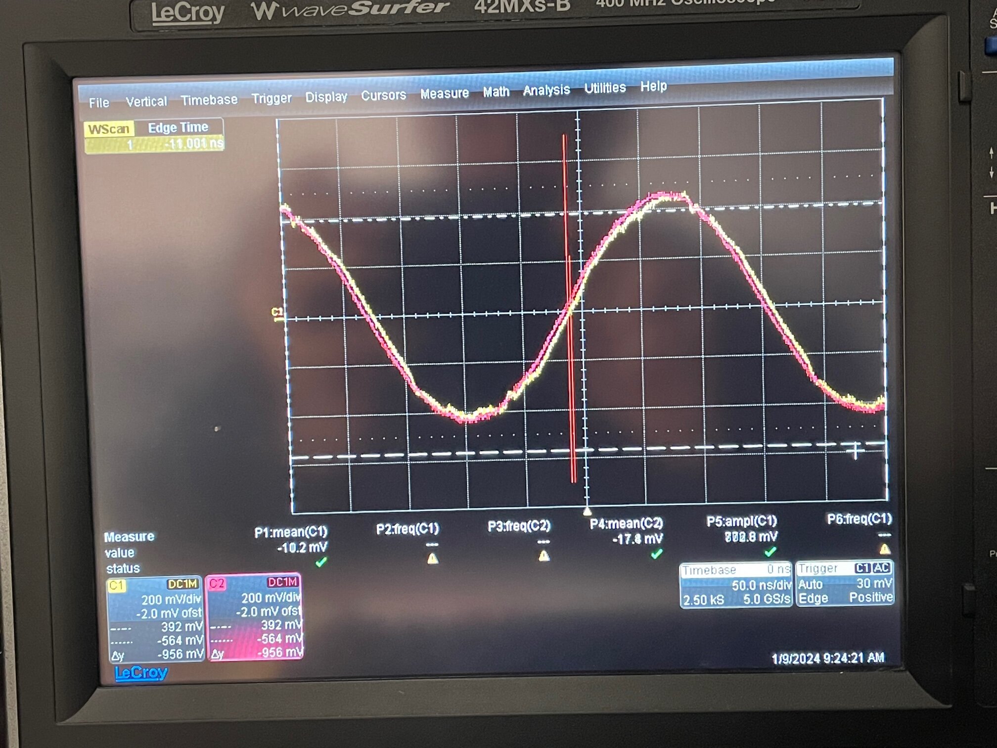
The signal going into all of the DG1208 pins isnt distorted and looks good at all frequencies (3MHz max is needed), but the signal on pin 8 above has some crossover distortion at all frequencies, and when you increase to frequencies above around 200kHz the distortion "moves" up the sinusoid .... see below
img_2956 : singals in (yellow) and out (red) of dg1208
img_2955 : closer look at the crossover distortion
img_2957 : another trace of showing the distortion
img_2958 : another look
img_2959 : Example of when frequency is significantly increased, the distortion moves along the wave, even past 90deg.
I am pondering what this is coming from, this is the first version of this board and imporvements will be made - but this distortion is baffling me a little....
The output load is minimal as the DG1208 is dirving a non-inverting buffer.... could this be the issue?
I really don't want to have to switch to using signal relays as i would need 6 and they are costly and large.
Any ideas on solutions to this would be most welcome!
I have a deisgn in which i have multiple signals entering a DG1208 mux.
I am using ada4807 op amps both before (to provide gain) and after (as a buffer) the DG1208.
At the output of the DG1208 pin 8 (COM) is a non-inverting buffer as follows;
The signal going into all of the DG1208 pins isnt distorted and looks good at all frequencies (3MHz max is needed), but the signal on pin 8 above has some crossover distortion at all frequencies, and when you increase to frequencies above around 200kHz the distortion "moves" up the sinusoid .... see below
img_2956 : singals in (yellow) and out (red) of dg1208
img_2955 : closer look at the crossover distortion
img_2957 : another trace of showing the distortion
img_2958 : another look
img_2959 : Example of when frequency is significantly increased, the distortion moves along the wave, even past 90deg.
I am pondering what this is coming from, this is the first version of this board and imporvements will be made - but this distortion is baffling me a little....
The output load is minimal as the DG1208 is dirving a non-inverting buffer.... could this be the issue?
I really don't want to have to switch to using signal relays as i would need 6 and they are costly and large.
Any ideas on solutions to this would be most welcome!