Continue to Site

Welcome to EDAboard.com

Welcome to our site! EDAboard.com is an international Electronics Discussion Forum focused on EDA software, circuits, schematics, books, theory, papers, asic, pld, 8051, DSP, Network, RF, Analog Design, PCB, Service Manuals... and a whole lot more! To participate you need to register. Registration is free. Click here to register now.

charge pump switch size choose problems

Status
Not open for further replies.

shirley070314

Newbie level 4
Joined
Mar 11, 2013
Messages
5
Helped
0
Reputation
0
Reaction score
0
Trophy points
1,281
Activity points
1,309
Hi, guys, I am designing a charge pump based PLL. and I have come across some problems that would like you to help me.

my problem is how to choose the size for switch in charge pump. I am using the tradtional charge pump circuits which includes UP and Down current source, PMOS and NMOS switch in the middle.

Icp=40uA/Process:0.18um / the charge pump output voltage range :0.8-1.5V

how could I choose the PMOS and NMOS size? anyone who have the experience please help me?
 

Hi,
Actually you have to fix the BW, Phase margine that you expects for your PLL. Ones this done you can calculate the required current for charge and discharge.
By knowing the process parameter K, Vth, .. you can easily determine the dimension of your transistor using the Ids equation.
 

Hi,
Actually you have to fix the BW, Phase margine that you expects for your PLL. Ones this done you can calculate the required current for charge and discharge.
By knowing the process parameter K, Vth, .. you can easily determine the dimension of your transistor using the Ids equation.

thank you for replying me. you point is right. but my problem is how to choose the switch size not the current source size. i know that my switch's Length can be 180nm, but how to determine Width of MOS? only the current 40uA is not enough to determine the size.
 

As you know you current that you want, you can choose value of W/L as you like provided W/L=Id/M

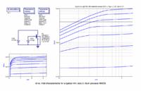
... and from the Id vs. Vdd characteristics of your process (simulate an NMOSFET) you can easily find out which W/L ratio is sufficient for your switch, see this example:
 

... and from the Id vs. Vdd characteristics of your process (simulate an NMOSFET) you can easily find out which W/L ratio is sufficient for your switch, see this example:

thank you so much. I will have a try

- - - Updated - - -

The equation of the current depends on the operation region in which the transistor is.
https://inst.eecs.berkeley.edu/~ee105/sp08/discussions/discussion9.pdf
Id=M*(W/L)

As you know you current that you want, you can choose value of W/L as you like provided W/L=Id/M

thank you . the link you sent me is really useful. I will have a try.
 

Status
Not open for further replies.

Part and Inventory Search

Welcome to EDABoard.com

Sponsor

Back
Top