Continue to Site

Welcome to EDAboard.com

Welcome to our site! EDAboard.com is an international Electronics Discussion Forum focused on EDA software, circuits, schematics, books, theory, papers, asic, pld, 8051, DSP, Network, RF, Analog Design, PCB, Service Manuals... and a whole lot more! To participate you need to register. Registration is free. Click here to register now.

Cascode amplifier

Status
Not open for further replies.

Sambhav_1

Full Member level 2
Joined
Jul 13, 2018
Messages
125
Helped
1
Reputation
2
Reaction score
3
Trophy points
18
Activity points
941
Hi,

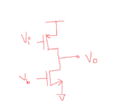
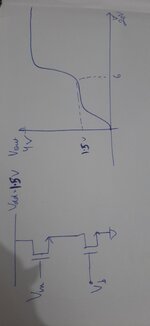
In the attached screenshot, vb is the fixed bias and vi is variable input to pmos and supply is vdd, what will happen if we sweep vi to infinite?how will the characteristic curve look like?
and what is we exchange the PMOS with nmos then how will the characteristic curve look like at vin = inf.

Thanks
 

Attachments

  • cascode.PNG
    cascode.PNG
    7.6 KB · Views: 108

1. I don't recognize a cascode amplifier.
2. Infinite voltage causes gate oxide and embedding air breakdown. Ask meaningful questions is you want useful answers.
 

1. I don't recognize a cascode amplifier.
2. Infinite voltage causes gate oxide and embedding air breakdown. Ask meaningful questions is you want useful answers.
can you simply analyze?what will happen if vi keeps on increasing? Does that sound reasonable?
 

vo decreases with increasing vi. vo is constraint to 0..vdd.
 

High side P type conducts less as you raise its bias voltage. (It shuts off when bias approaches supply voltage.)

High side N type conducts more as you raise its bias voltage.
 

High side P type conducts less as you raise its bias voltage. (It shuts off when bias approaches supply voltage.)

High side N type conducts more as you raise its bias voltage.
Here vdd is kept as 1.5 and sweeping vin from 0 to20v, (this is just an experiment i am doing for curiousity) i am seeing the cirve shown in the attached file. after certain voltage it is rising sharply and then keeps settled for any vin. it might be due to the breakdown of top nmos or any other reason but i dont know why this settling to a higher voltage.
 

Attachments

  • 16217072370193375572563446457795.jpg
    16217072370193375572563446457795.jpg
    606.8 KB · Views: 114

With a bjt there are two internal diodes which the bias can go through. Normally it only goes through the emitter diode.

However your experiment applies bias voltage which overcomes the supply voltage at the collector. Current travels up in reverse direction to the power supply. It's an abnormal method of using a bjt therefore the output is abnormal.

As for mosfets... They do not act exactly the same way as a bjt. They might have different threshold bias voltages which must be reached before they start to turn on. They have a body diode which we must take into account.

If the mosfet is healthy mosfet then it responds to bias voltage but its insulated gate does not pass current. However if the gate has been perforated then the device acts abnormally. Mosfets are sensitive to being ruined by static charge, and even 40 or 50 volts could be sufficient to alter its operating characteristics permanently.

You didn't make it clear whether your circuit is hardware or simulated. It might help if you run tests on your transistors individually, in the most basic circuits which demonstrate how it performs over a normal range of bias and supply voltages.
simulated one
 

As stated in post #4, vo is constrained to Vdd (1.5V) in normal operation. Rise above Vdd is only possible due to gate oxide breakdown and involves permanent damage. The purpose of your experiment is unclear.
 

Status
Not open for further replies.

Part and Inventory Search

Welcome to EDABoard.com

Sponsor

Back
Top