Continue to Site

Welcome to EDAboard.com

Welcome to our site! EDAboard.com is an international Electronics Discussion Forum focused on EDA software, circuits, schematics, books, theory, papers, asic, pld, 8051, DSP, Network, RF, Analog Design, PCB, Service Manuals... and a whole lot more! To participate you need to register. Registration is free. Click here to register now.

[SOLVED] Calculate values in an amplifier

Status
Not open for further replies.
So it should be R4=(12-5.16667)/0.004=1708.3325Ω

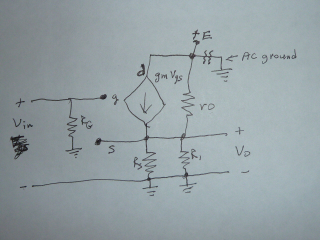
So if I get you right I should take the derivative of iD=IDSS*(1-uGS/Up)² with respect to uGS.

With the given values inserted this equals: 0.00514286+0.00146939uGS, when I put my uGS in it, it gives me gm=0.00342857=3.4286mS

Haha, it's the same(but positive)! Sick!

How do I calculate the operating point of the first FET?
 
Last edited:

How do I calculate the operating point of the first FET?

You find a ugs such that the current resulting from that ugs causes a voltage drop across Rs which is equal to said ugs.

Then you plug that ugs into the expression for gm.
 
You find a ugs such that the current resulting from that ugs causes a voltage drop across Rs which is equal to said ugs.
To get the exact bias point, you have to solve a quadratic equation. Or solve it iteratively, starting with Vgs = Vp.
 
I read at a FET biasing page;
The operating point (that is zero signal ID and VDS) can easily be determined from equation and equation given below :
VDS = VDD – ID (RD + RS)


Where my values are; VDD: 10V ID=IDSS=9mA RD=2kΩ RS=15kΩ

VDS=10-(9*10-³)*(2000+15000)=-143V

0.00514286+0.00146939VDS=-0.20498S

Btw, why am I doing this, because as I see it, my values for R1, R3 and R4 are already calculated and should suffice for an answer in the a section. Or maybe we have ventured into the b section already?

-------------------------

Attention, I realize that this isn't correct. Im now trying to find an UGS in the way The Electrician said, but this is taking some time.
 
Last edited:

I read at a FET biasing page;
The operating point (that is zero signal ID and VDS) can easily be determined from equation and equation given below :
VDS = VDD – ID (RD + RS)


Where my values are; VDD: 10V ID=IDSS=9mA RD=2kΩ RS=15kΩ

VDS=10-(9*10-³)*(2000+15000)=-143V

0.00514286+0.00146939VDS=-0.20498S

You know this can't be right because your supply voltage is only 12 volts; how could you have -143 volts across the FET?

Looking at the circuit, we see that the voltage across Rs is the same as the voltage UGS, with a sign change.

We know that iD=IDSS*(1-UGS/Up)² for a particular value of UGS. The voltage across Rs is then given by Rs*IDSS*(1-UGS/Up)² which must equal -UGS.

Substitute numerical values for everything but UGS and solve this equation:

Rs*IDSS*(1-UGS/Up)² = -UGS

Only one of the roots makes sense.

Btw, why am I doing this, because as I see it, my values for R1, R3 and R4 are already calculated and should suffice for an answer in the a section. Or maybe we have ventured into the b section already?

Yes, this is needed for the b section.
 

Yes, ofcourse I realized this wasn't correct. I just got so frustrated that I couldn't come up with a answer that makes sense that I left it there.

Rs*IDSS*(1-UGS/Up)²=-UGS, Where Rs=15kΩ IDSS=9mA Up=-3.5V

<=> 15000*(9*10^-3)*(1-(UGS/(-3.5)))^2=-UGS, I get two values; UGS1= -4.111V UGS2= -2.98V


Trying to determine which one makes sense, I'm looking at this image in my book, and I guess that UGS2 makes the most sense..

ugs.jpg

With UGS=-2.98V in 0.00514286+0.00146939uGS = 0.0007640S = 0.7640mS

And with UGS=-4.111V I get negative slope which I don't recognize i've seen before.
 

The pinch-off voltage is -3.5 volts. Any voltage below that will turn off the FET and there won't be any drain current at all. That's why UGS1 doesn't make sense.

Now you have to draw 3 small signal models for each stage of the circuit. Wikipedia has models for the FET stages:

https://en.wikipedia.org/wiki/Common_gate

https://en.wikipedia.org/wiki/Common_source

The common gate page has formulas for impedance and gain that involve a parameter designated as gmb. This is the body transconductance and doesn't apply to a JFET like you have, so just remove it from the formulas if you use them, which you shouldn't need to because you'll be doing your own analysis.

You should be able to find a model for a BJT in your textbook.

The 3 models are connected together of course. Once you have them properly set up you can solve the network using nodal analysis. Let the input be driven by a 1 volt test signal and solve for the output voltage; this will give you the voltage gain of the circuit.
 

Well, after watching some videos about makin a small signal model, the model for the common source transistor should be like this:

commonsource.png

I'm working on the rest as we speak..

Here is the final schedule we got;

uppg3värden.png

----------------------------------

Not entirely sure about the small-signal model of the common-gate, but here goes nothing.

commongate.png

- - - Updated - - -

And here is the common emitter:

commonemitter.png

The equivalent small-signal model:

commonemitter2.png

Wow, I'm really not sure if these are correct at all!
 
Last edited:

Why is the transistor biased so that it is almost cutoff?
Why is the value of the emitter resistor so high that if the transistor is biased correctly then you are throwing away most of the output voltage swing?

I simulated your circuit. Its collector voltage idles at about +10.7V and its emitter about +1.7V.
Believe it or not the input is a perfect sinewave with a peak voltage of only 40mV. The output is so distorted that it does not look like a sinewave and its amplitude cannot be measured.
 

Attachments

  • transistor.png
    transistor.png
    22 KB · Views: 89

Don't forget that's it's an excercise problem rather than a real amplifier design. Post #1 says the input voltage is only 1 mVpk.
 

There are 3 active devices in this circuit, and each has a different transconductance, so let's use gm1, gm2 and gm3 for the three gm values.

Well, after watching some videos about makin a small signal model, the model for the common source transistor should be like this:

View attachment 110655

The first FET is in a common drain topology, not common source. There's a resistor RD between the drain and AC ground, but it shouldn't affect the small signal performance; we'll still use a common drain model, but with RD in between drain and ground. If there were a resistor for the FET's internal resistance (ro), leaving RD in place would affect performance, but your problem says to neglect the FET output admittance ro.

Not entirely sure about the small-signal model of the common-gate, but here goes nothing.

View attachment 110657

This model looks ok, but eliminate the 1/gm resistor. Change the label to the right of the 1/gm resistor to Vs rather than Vgs. Move the R1 resistor to where the 1/gm resistor was. The input goes directly to the source of the FET.

The dependent current source should be in a diamond shaped box, not a circular box. The arrow should point to the right, and the control expression should be gm2*Vs.

And here is the common emitter:

View attachment 110658

You have no controlled source in this model, so it won't work. Use the model from Figure 1 on this page: https://en.wikipedia.org/wiki/Hybrid-pi_model
but leave out ro. Denote the transconductance in this model as gm3.

You will need to calculate gm3 for the BJT.

To make it easier to communicate about the final circuit, label the nodes of the overall circuit like this:

Node 1 = gate of FET1
Node 2 = drain of FET1
Node 3 = source of FET1 and source of FET2
Node 4 = drain of FET2 and base of BJT
Node 5 = collector of BJT

In the nodal equations you will have to develop, v1 will be the (small signal) voltage at node 1 (with respect to ground), v2 will be the voltage at node 2, and so forth.
 

I tried to do as you told me, regarding the BJT and so on. I just want to have it confirmed that the small-signal models are correct, before labelling the nodes.

Common-drain
commonsource.png

Common-gate
commongate.png

Common-emitter
commonemitter3.png
 

To try and answer your question, this is a school exercise and this amplifier will not be built.

If you're irretated that the circuit doesn't make any sense, be mad at my teacher! ;-)
 

Normally the model for a common drain JFET would be this:

2791839100_1414204040.jpg


But since your problem says to neglect ro, and the drain of FET1 is not connected directly to +E, but rather through a resistor RD, we need to modify the model a bit to this:

6284427200_1414204171.jpg


This creates another node, #2, which will allow us to determine if the presence of RD affects the performance of the circuit.

Don't label the controlling variable of the dependent current sources Vs for all three models. That label is appropriate for the common gate model, but not necessarily for the others.

In these models of the individual stages, sometimes resistors are shown as loads on a given model, and also on a following model. This will allow us to get an approximate figure for the gain of a particular stage, but when all three models are connected together, we must be careful not to duplicate any resistors.

Your common gate model looks OK.

Your common emitter model is not correct. I'll post a good version in a while.

- - - Updated - - -

In post #27, I included a link to a common source model; it should have been a link to a common drain model:

https://users.ece.gatech.edu/mleach/ece3050/notes/mosfet/cdamp.pdf

- - - Updated - - -

Use the model shown in Figure 1 on this page for the BJT common emitter model:

https://en.wikipedia.org/wiki/Hybrid-pi_model

Get rid of ro, and label gm as gm3. RE should not be present in the model because it is bypassed by a large capacitor; this means that the emitter is grounded for small signals. Rc and RL are in parallel, connected from the collector to ground.

Remember that anything connected to +E is effectively grounded for small signals.
 
Alright, common gate is fine.

Then I have remade the common-drain according to your drawing:

commondrain.png

And then the common-emitter:

commonemitter4.png

- - - Updated - - -

Maybe the VGS should be Vbe in the common-emitter.

- - - Updated - - -

Here are the small-signal models with the nodes numbered:
Common-drain
commondrain.png

Common-gate
commongate.png

Common-emitter
commonemitter4.png
 
Last edited:

The BJT model is incorrect; it should be like this:

3223893800_1414249315.jpg


Note that Vin is the same as Vbe for this model. I didn't include the node numbers, but you got those right.

You will need to calculate Rpi for the BJT. R5 and R6 make up a voltage divider to provide the base bias. The β for this BJT is 100, so we can probably ignore the base current effect on the voltage divider; the voltage at the base then will be 12*(10/(10+40)) = 2.4 volts. Allowing Vbe to be .6 volts, this gives us 1.8 volts across RE, and the DC emitter current is 2000/1.8 = .9 mA; finally, re is 25 mV/.9 mA = 27.77778 ohms. From this we get Rpi = (β+1)*re = 2805.5556 ohms and gm3 = β/Rpi = .0356436

The problem statement in post #1 says the input impedance of the BJT is 1.5 kΩ, which is quite different from the calculated value; do you know why it is so different?

When you connect these three models together, don't duplicate any resistors. R1 is present in the first and second models; only include it once in the combined circuit. Also, R5 and R6 are in both the second and third models; only include them once in the combined circuit.

Put all the models together, showing the node numbers. Remember when setting up the nodal equations that the voltages at the nodes are: v1 at node 1, v2 at node 2, v3 at node 3, etc.

In the common drain model the control expression is gm1*vgs; in the complete model it will be gm1*(v1-v3) because vgs = (v1-v3).

In the common gate model gm2*vs becomes gm2*v3. In the common emitter model, gm3*vbe becomes gm3*v4.
 
Sorry for taking so long.
I honestly have now idea why the given value and the calculated value differs so much. Is the problem faulty or have I made a mistake along the way?

This is the connected small-signal model we got;

alltogether.png

With the values: RG=1MΩ RS=15kΩ RD=2kΩ R1=791.7Ω R4=1708.3Ω R5=40kΩ R6=10kΩ RΠ=2805.6Ω RC=3kΩ RL=2kΩ

gm1=0.0007640S gm2=0.00342857S gm3=0.0356436S

I'll start doing my nodal analysis now.

- - - Updated - - -

I should be able to simplify the model a little bit..

1/Rtotal(3)=1/RS+1/R1 => 1/Rtotal(3)=1/15000+1/791.7 <=> Rtotal(3)=752Ω

1/Rtotal(4)=1/R4+1/R5+1/R6+1/RΠ => 1/Rtotal(4)=1/1708.3+1/40000+1/10000+1/2805.6 <=> Rtotal(4)=937.376Ω

1/Rtotal(5)=1/RC+1/RL => 1/Rtotal(5)=1/3000+1/2000 <=> Rtotal(5)=1200Ω


alltogether2.png
 
Last edited:

It all looks good, assuming neither one of us has made a mistake. :cool:

Sorry for taking so long.
I honestly have now idea why the given value and the calculated value differs so much. Is the problem faulty or have I made a mistake along the way?

Our calculation of the biasing of the BJT is correct, AFAIK.

I also noticed that in post #1, the problem said about the FET that "Slope: 4mS". I wonder what that means? The gm for the two FETs is not the same, and neither one has a gm of 4 mS according to the calculations so far.

If you set up your nodal equations as input to a solver in Matlab, you can easily change rpi to be 1.5kΩ instead of the calculated 2805.56 Ω and get a solution with that value.

Do you have an instructor for this course, or is it an online course? If you have an instructor it would be interesting to ask about these questions.

I'm curious to know what software you're using to create your model drawings; it looks very good.
 
I do have an instructor for this course, and I will ask him about this, but he won't reply until monday. The slope is the gm-value for the transistor.

Maybe, we should have assumed the gm-value was 4ms for both of the transistors, but I don't know for sure.

So, should I begin my nodal analysis now?
 

Status
Not open for further replies.

Part and Inventory Search

Welcome to EDABoard.com

Sponsor

Back
Top