Continue to Site

Welcome to EDAboard.com

Welcome to our site! EDAboard.com is an international Electronics Discussion Forum focused on EDA software, circuits, schematics, books, theory, papers, asic, pld, 8051, DSP, Network, RF, Analog Design, PCB, Service Manuals... and a whole lot more! To participate you need to register. Registration is free. Click here to register now.

How to calculate differential pair target Zdiff?

Rimvis123

Junior Member level 2
Joined
Oct 30, 2023
Messages
22
Helped
1
Reputation
2
Reaction score
0
Trophy points
1
Activity points
202
hello everyone,

I do not understand how to calculate diff pairs with saturn or Sierra circuits programs. I need to route 100ohm (this line is from crystal oscillator to microcontroller so 100 ohm is right yes?) impedance diff pair line. I'm trying to calculate it, but I don't understand what dielectric height, ΔW and Trace Thickness (T) ( mm ) I need to put. In dielectric height I need put 1,6mm as my full pcb height or height between top and second layer?
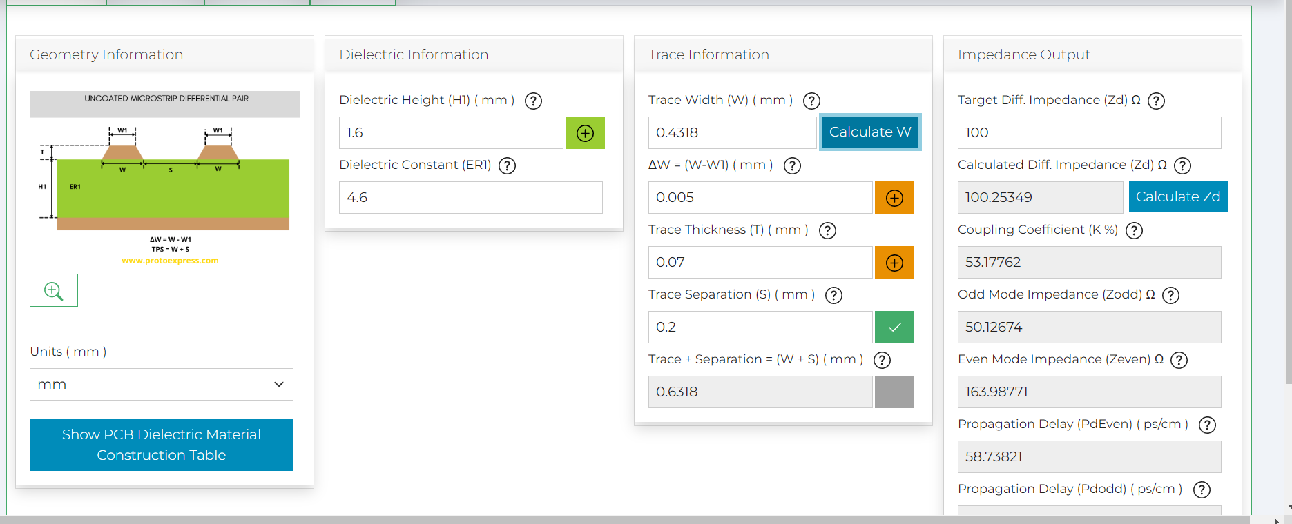
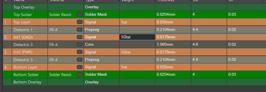
1708093263230.png


1708093399729.png
 
You may not need a differential impedance or a coplanar waveguide or even a controlled impedance.
Is the path length < 1/20 wavelength?

e.g. if the XO was 350 MHz your max trace length is likely greater than your trace.

Even if your rise time was 1 ns = tR (or Sr in Saturn) usin 1/4 Sr for the spectral content of significant harmonics is slower than the propagation delay of 35 mm , so does this make sense? It means the echos are faster than the risetime for a few mm trace length, so any short single trace will work fine from an active XO (Crystal Oscillator)
 
Last edited:
My path lenght (if I understand that correctly) is shown in picture below. And my crystal oscillator is 32MHz. So in this case my max trace lenght is more than enough, yes?

1708095112898.png
 
My path lenght (if I understand that correctly) is shown in picture below. And my crystal oscillator is 32MHz. So in this case my max trace lenght is more than enough, yes?

View attachment 188660
Why don’t you flip the oscillator around to shorten the path?

But to answer your original questions, just look at the diagram YOU posted. Dielectric height is the height between the trace and plane. Trace thickness is, um, the thickness of the trace.
 
Why don’t you flip the oscillator around to shorten the path?

But to answer your original questions, just look at the diagram YOU posted. Dielectric height is the height between the trace and plane. Trace thickness is, um, the thickness of the trace.
1. It need to be in this possision. It's not my own pcb, I just need to calculate things that I asked in this post, so original owner said, that this need to be like this.
2.Dielectric height - is 0,2104mm?
3.So that i choose 0.07 is good?
 
This is what we call an XY question. TS assumes the problem which is not the problem.

You assumed controlled impedance was the problem and is an XO = active crystal oscillator. But it is neither true for this.
It is just a passive crystal, X not an active device but passive with load C's C35 and Cxx hidden.

Worse yet, the 1st X he chose , uses 2 pins in a non-std adjacent pads
Seiko Epson
1708099959938.png


While most X SMDs are diagonal corners with opposite diagonal corners connected to Gnd such as your alternate NDK P/N which will fail.

ECS, NDK, Kyocera, NDK etc

1708100050934.png


This means you will have a hard time finding an alternate source from Seiko's non-std pads.

So what is your real problem? To me it looks like a design problem with no second source using a unique pad layout from Seiko..
 
Last edited:
So i should not use both C's with this XO? And overall I need to use different XO? Sorry for questions, but it's first my and my friend bigger project.
 
You can only use the Seiko X part in this design, which locks you into one source.

The diagonal corner pins for a shorter Crystal is more the "defacto std." with many sources.

It also means for this problem Controlled impedances is irrelevant on diff traces but the value of C is critical for accuracy. 12.5 pF std load means the two caps equivalent series Ceq is 12.5 so 1/25 pF + 1/25 pf = 1/12.5 pF
 
You said here it is a 32 MHZ oscillator yet your 1st link it points to a tuning fork 32 kHz Crystal

Now it starts to make sense.

Don't worry we all make rookie misteaks. XO is active . This design is passive X , the active part is in the uC.

32.768k Crystals have a different defacto layout than MHz Quartz crystals
So there are alternate sources
1708101401824.png


These crystals use different pads and different pF load, so do not substitute unless you can live with 1 second timing clock error due to wrong C load caps.

The 32 MHz uses pin 1,3 with 2,4 grounded
the 32.768 kHz uses pin 1,2 with 3,4 floating. but if you read the datasheet, some use different pin numbers like 1,4 for tuning fork 32.768 kHz so pay attention to details. There is no design reason why this 32 kHz xtal could not have been flipped around and that is the reason why it is at one end to be close to the caps and uC and eliminate parasitic traces which add 3 pF/cm like in his design. That part you can verify in Saturn using no ground plane. or large gap . Also he should never run signal traces under crystal signals on top for this causes crosstalk and affects SNR of clock. Maybe ok, may not.

1708101661993.png


1708102157709.png


if you want an accurate clock for timing errors in < 10 ppm , he should have chosen an XO rather than a passive X + 2 caps. XO's are designed to be more accurate. e.g. https://www.mouser.lt/datasheet/2/137/TG_3541CE_en-1601070.pdf 1.9 ppm 0 to 50'C TCXO here

That is my final recommendation on this XY question. But if ppm error not an issue, what you have may work. Just don't mix X with XO and kHz and MHz.
 
Last edited:

LaTeX Commands Quick-Menu:

Part and Inventory Search

Welcome to EDABoard.com

Sponsor

Back
Top