Continue to Site

Welcome to EDAboard.com

Welcome to our site! EDAboard.com is an international Electronics Discussion Forum focused on EDA software, circuits, schematics, books, theory, papers, asic, pld, 8051, DSP, Network, RF, Analog Design, PCB, Service Manuals... and a whole lot more! To participate you need to register. Registration is free. Click here to register now.

CADstar PCB questions

Status
Not open for further replies.

bmmm

Newbie level 3
Joined
Aug 24, 2011
Messages
3
Helped
0
Reputation
0
Reaction score
0
Trophy points
1,281
Activity points
1,315
Hello,

I am laying the PCB in CADstar 12.1 Express. As a beginner, I need help on the following questinos:
1)how can i set the copper trace width of a signal (eg: VCC, GND, etc)? Is there a quicker way than setting the width manually in every connection?

2)How can I specify the V-grooving and CNC routing of the PCB? Which layer should I draw the v-groving traces on? Which layer should I draw the CNC route on?

3)If I dont want the ground plate automatically connects to the un-connected pins, where can I configure this?

4)In PCB routing, when I am routing a trace between two pin, why the trace can only exiting the pad from two directions only? ie (can only go East or West in fig1). To have more flexibility in routing, the trace exiting from the square pad should be able go in any direction. What have I done wrong?
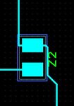
fig1_no_go_north.JPG


Thank you!

Q
 

1.) use classes on schematic, this way you can set trace widths according to class on your pcb. If you know your commands you can easily switch your trace widths on your pr editor

2.) never heard of v grooving before and cnc route as well.sorry can't help you on this one

3.) that never happened to me before.

4.) check your routing angle...i believe it can be set from 90, 45 and even 180. also check your routing topology but i'm not sure if cadstar has that feature.

if all fails press f1.. ;)

is used cadstar 11 previously not sure if cadstar 12 have the same features
 

Milling contoures are usually extracted from the board outline, I assume, that inner cutouts can be added here with Cadstar.
Other mechanical features like V-groove should be defined on a separate mechanical layer.
 
  • Like
Reactions: bmmm

    bmmm

    Points: 2
    Helpful Answer Positive Rating
1) There is no quicker way to change route codes on nets than selecting them.

However, using Edit\Net Tools\Select Net you can group select many nets and then choose their properties to change the net route code.

Also, before you start the schematic, set the Settings\Defaults\Connection route code, this will be the route code used as default
for all signals until you set them as something else. As the majority of connections are left at default widths then only those that need to be different need selecting and changing.

Or when adding the nets you can change the default to something else and any nets added will then be the new default.

Personally I find it quicker to add all nets at default then change them afterwards.

(ISTR There is another way using the attribute editor and adding a width attribute - but this is more work and hassle than simply selecting and setting the widths.

2) Either create a new documentation layer or use the "Letter Drill Drawing" layer. Often additional layers are created for scoring and routing information.

3) not so sure what you mean, can you please try and explain this further?

4) when you start routing, RMB and deselect "Restricted Exit".
The system is setup to use exit directions on pads to control the autorouter (and manual routing) so that it does not route from the pads in the wrong direction (set when the component is created) and this can be turned off when you first start manual routing.
It defaults to the shortest side of a rectangular pad, unfortunately this means a resistor is exited at the sides so edit your 2 terminal SMT components so that the default exit direction is N/S instead of E/W.

---------- Post added at 23:30 ---------- Previous post was at 23:16 ----------

Edit - for no.3 - the groundplane will not connect to any pins of any nets that are not part of the groundplane.

I suggest you do not use a powerplane but instead have your ground layers set as electrical and use a template and pour copper in that within the route editor.
 
  • Like
Reactions: bmmm

    bmmm

    Points: 2
    Helpful Answer Positive Rating
For v GROOVE OR CNC milling create a leyer exclusively for the data just for these functions. V-groove will be just straight lines, it is important to specify minimum web and angle of v-groove. CNC, I recreate the exact cutting path (paths) I wont, representing them graphicly using a line width of the same size as the diameter of the tool I wont the manufacturer to use, I can then see any problems and easily add brealouts etc. This I do in 2D CAD and import to Cadstar as a DXF.
Create macros to change track widths then add these as a macro toolbar, set it up on all systems then as engineers add connections they can add it with the right track code adding more valuable information to the schematic?layout interface.

---------- Post added at 10:25 ---------- Previous post was at 10:23 ----------

Lost_dude, how would you route 2 segments 180 degrees to each other:smile:

---------- Post added at 10:33 ---------- Previous post was at 10:25 ----------

V-groove angle, as the tool used to create the v-groove wears down the angle increases usualy within the range 30-45 deg, as the angle increases the gap at the top of the cut gets wider, this can cause problems on dense boards, and make it harder to get good registration when using the "bacon slicer" to de-panelise the PCB.
Personaly I hate v-groove, it is one of the most inaccurate and stressfull (for the components) ways to de-panelise PCB's. It does have its place though, for the lower end of designs, I've designed numerous PCB and panel schemes that have used v-groove, and experimented both with panel sizes etc to get the most out of this method of de-panelising.
The WEB thickness is how much PCB material is left after the v-grooves have been cut, to little and the panel will sag through the various heat profiles during assembly, to thick and the de-panelising bacon slicer will either not register or strugle to cut the remaining material.
 
  • Like
Reactions: bmmm

    bmmm

    Points: 2
    Helpful Answer Positive Rating
Status
Not open for further replies.

Part and Inventory Search

Welcome to EDABoard.com

Sponsor

Back
Top