bestvlsi
Junior Member level 1
Hi All,
I am doing layout for an NMOS differential pair with PMOS active load . The differential pair layout has passed the DRC and LVS. The PMOS active load has passed the DRC but is stuck with LVS.
The problem I am facing in LVS is that its throwing up an error that the width of one of the devices is more than that of the other.
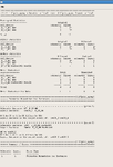
After checking the log file i found that in Reduce statistics Cadence has reduced the number of PMOS transistor to 1.
Reduce Statistics
================= Filtered Reduced
Cell/Device schematic layout schematic layout
(N_18_MM) MOS 2 4* 2 2
(P_18_MM) MOS 3 5* 1 1
(P_18_MM arMos2#1) MosBlk - - 1 1
Also there is 1 PMOS used for powerdown facility in the current mirror load.

Now each of the PMOS and NMOS device has 2 fingers as well as 2 dummy for the differential pair and active current mirror load, respectively . Now why does the reduced schematic has only 1 PMOS transistor instead
of 3 ( the 2 active loads and 1 power down) .
Also the log file is as given in the attachment below.
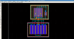
And the layout is shown in the attachment.
Regards.
I am doing layout for an NMOS differential pair with PMOS active load . The differential pair layout has passed the DRC and LVS. The PMOS active load has passed the DRC but is stuck with LVS.
The problem I am facing in LVS is that its throwing up an error that the width of one of the devices is more than that of the other.
After checking the log file i found that in Reduce statistics Cadence has reduced the number of PMOS transistor to 1.
Reduce Statistics
================= Filtered Reduced
Cell/Device schematic layout schematic layout
(N_18_MM) MOS 2 4* 2 2
(P_18_MM) MOS 3 5* 1 1
(P_18_MM
arMos2#1) MosBlk - - 1 1Also there is 1 PMOS used for powerdown facility in the current mirror load.
Now each of the PMOS and NMOS device has 2 fingers as well as 2 dummy for the differential pair and active current mirror load, respectively . Now why does the reduced schematic has only 1 PMOS transistor instead
of 3 ( the 2 active loads and 1 power down) .
Also the log file is as given in the attachment below.
And the layout is shown in the attachment.
Regards.
Attachments
Last edited: