Continue to Site

Welcome to EDAboard.com

Welcome to our site! EDAboard.com is an international Electronics Discussion Forum focused on EDA software, circuits, schematics, books, theory, papers, asic, pld, 8051, DSP, Network, RF, Analog Design, PCB, Service Manuals... and a whole lot more! To participate you need to register. Registration is free. Click here to register now.

Cadence - gain and phase plot

Status
Not open for further replies.

astroshey

Newbie level 6
Joined
Nov 21, 2021
Messages
12
Helped
0
Reputation
0
Reaction score
0
Trophy points
1
Activity points
106
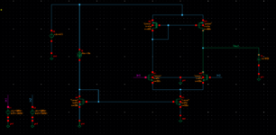
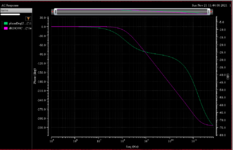
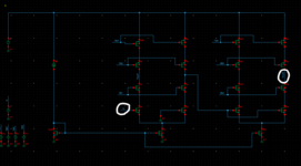
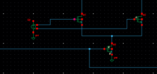
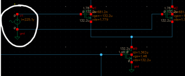
Hi, I am new to cadence and I am designing a differential amplifier. I am trying to find the gain bandwidth product. My phase and gain plot looks wrong as both gain and phase curves start at 0deg. Can someone please suggest what might potentially be wrong? I have a attached my plot and schematic if that helps. Thank you
 

Attachments

  • DiffAmp_schem.PNG
    DiffAmp_schem.PNG
    18.9 KB · Views: 259
  • DiffAmp_gainphase.PNG
    DiffAmp_gainphase.PNG
    55.3 KB · Views: 265

You are plotting common mode instead of differential gain, same voltage applied to both inputs. That's why you see negative gain. And your measurement circuit has apparently no provisions to stabilize the operation point, can't see if it is set appropriately.
 
Thank you for getting back. I am still very confused about how to probe differentially in cadence. Current I am probing at the circled pins - see attached. My goal is to get a GBW of 200GHz. I have a feeling that the way I am probing is still wrong. Please can anyone tell me (keeping in mind that I am a rookie) exactly how to probe differentially. Much appreciate any help. Thank you
 

Attachments

  • twostagecascode_schem.PNG
    twostagecascode_schem.PNG
    32 KB · Views: 130

To convert difference signals to a single ended
ground referred difference voltage, use a vcvs
(control inputs to the signals of interest, output
from gnd (0 node) to a "vdiff_in" node you can
plot and measure neatly; similarly for differential
output).

You can then plot gain and phase of these
differential quantities, from their single-node
"proxies".
Thank you very much for getting back. I added a vcvs but I am not sure about how to connect it (see image 1) - not sure about the top pin, where should that go? So, then I opted for an AC source instead (image 2). But for some reason that makes my gate voltage at MOSFET M1 zero. I am still struggling with changing my differential input to be summed and single. Any help is appreciated, thank you.
 

Attachments

  • 1.PNG
    1.PNG
    4.3 KB · Views: 121
  • 2.PNG
    2.PNG
    16.9 KB · Views: 125

Status
Not open for further replies.

Part and Inventory Search

Welcome to EDABoard.com

Sponsor

Back
Top