godfreyl
Advanced Member level 5
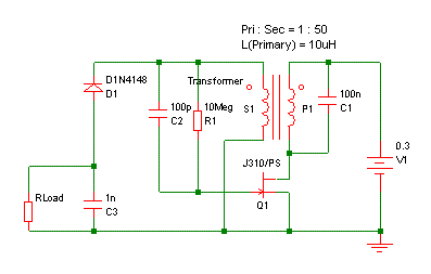
The amplitude of oscillation is limited by the fact that the gate draws current when it is more than about 0.5V positive, relative to the source.
If you can get the circuit to oscillate, the amplitude can be increased by adding a high value resistor, bypassed with a capacitor, in series with the gate. This allows the gate to float to a negative voltage, allowing greater voltage swing.
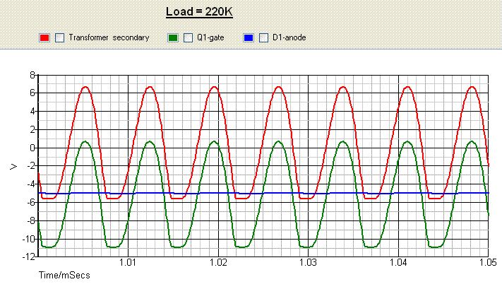
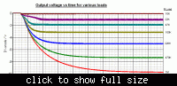
I got the results below in a simulator. Reality is always different, but it does look encouraging.
If you can get the circuit to oscillate, the amplitude can be increased by adding a high value resistor, bypassed with a capacitor, in series with the gate. This allows the gate to float to a negative voltage, allowing greater voltage swing.
I got the results below in a simulator. Reality is always different, but it does look encouraging.