Continue to Site

Welcome to EDAboard.com

Welcome to our site! EDAboard.com is an international Electronics Discussion Forum focused on EDA software, circuits, schematics, books, theory, papers, asic, pld, 8051, DSP, Network, RF, Analog Design, PCB, Service Manuals... and a whole lot more! To participate you need to register. Registration is free. Click here to register now.

Boost Converter Design and Output Current Problem

Status
Not open for further replies.

recon1729

Newbie level 4
Joined
Mar 22, 2012
Messages
6
Helped
0
Reputation
0
Reaction score
0
Trophy points
1,281
Activity points
1,331
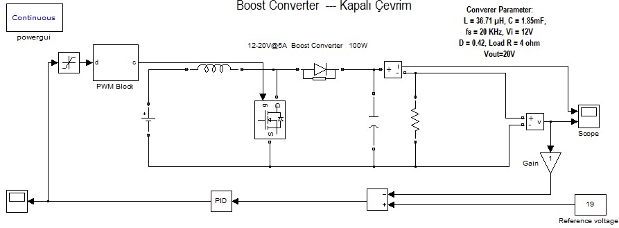
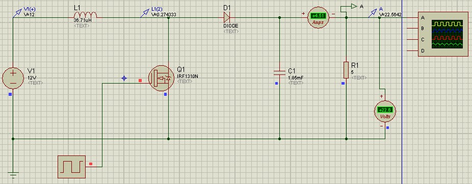
Objective: Design a Boost Converter with this spec :

Vi=12V
Vo=19V
Io=4.7A
P=90W
D=0.37
f=20kHz

For my calculation

L=36.71e-6
C=1.85e-3

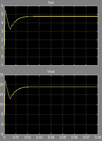
Then i simulate the circuit in both MATLAB and PSIM and i get the voltage just around 2A !!!
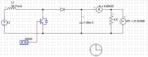
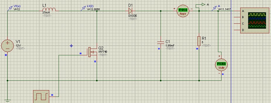
PSIM image
boost.jpg

So, how i get the 4.7A as output?.i try the change D but with this both voltage and current are rising.Please help!
 

i get the voltage just around 2A !!!
Dear recon
Hi
What do you mean by that ?!
And do you know the formula of out put voltage of boost converter ? and how you designed the L and c and what is your frequency ?
I have some doubt about the values . and about the duty cycle .
Best Wishes
Goldsmith
 

I wonder, how you want to achieve 4.7 A at 19 V with 10 ohm load?
 

You need this :
95-watt Laptop PSU Adaptor
12 V in, 19 V at 5 A out!
**broken link removed**


I never liked simulators.
 

I'm in a hurry, sorry for my bad english :)


Thanks for replies

@FvM:Thanks for the remembering basic electric laws :), now i change the load and i get the desired current value.


@goldsmith:Thanks , for first time the output current nearly reach 2A because of the load.Now problem is solved.And equation i use from Prof. Ali Keyhani and other common equations and they works.I have wrote the frequency as f=20kHz, maybe you miss it.

The purpose of the circuit for charging Laptop(notebook) battery.The common output for this 19V@4.7A.I design for University Project.
 

In a real design, you'll use a voltage control loop rather than precalculated duty cycle. This is necessary to keep the voltage constant when changing to DCM operation at low load currents and also to compensate for various effects like inductor series resistance or switch saturation voltage.
 

@FvM:Thanks for efforts, Now i build the circuit in Simulink, I have PID feedback too.Everything is OK.
Simulink images


28_1332668451.jpg


Next step is building the circuit in Proteus and getting the PCB scheme.I built circuit but the values is not same with Simulink's Values.I add the image below.


Whats wrong in the circuit.L and C values is the same with Simulink values.Can you help me again?

Best Regards...
 

I'm not using Proteus, but he voltage and current levels seem to show the initial transient solution rather than an average values in transient analysis steady state. You should check the transient analysis waveforms.
 

@FvM: I found the solution :) .The trick is selecting the suitable MOSFET type.Because of the saturation, first FET was not enough for me.Then I select the FET with their Power , voltage and current valuees.I found the IRF1310N.Now circuit works like my simulink model.

Here is image


Now i should drive the mosfet with a PIC.Like this


I must write a code.Can you help me a bit?
 

The purpose of the circuit for charging Laptop(notebook) battery.The common output for this 19V@4.7A.I design for University Project.
Please be careful in designing when the laptop battery is lithium. I am not sure the boost converter is solution for that.
 

Status
Not open for further replies.

Similar threads

Part and Inventory Search

Welcome to EDABoard.com

Sponsor

Back
Top