Continue to Site

Welcome to EDAboard.com

Welcome to our site! EDAboard.com is an international Electronics Discussion Forum focused on EDA software, circuits, schematics, books, theory, papers, asic, pld, 8051, DSP, Network, RF, Analog Design, PCB, Service Manuals... and a whole lot more! To participate you need to register. Registration is free. Click here to register now.

Bandgap design, find a ratio for the resistors.

Status
Not open for further replies.

vadim888

Member level 2
Joined
Feb 4, 2013
Messages
46
Helped
5
Reputation
10
Reaction score
5
Trophy points
1,288
Activity points
1,596
Hi all,

I am designing a bandgap, and I have a question. I want to find a proper ration for these resistors, and have no idea how to star...

Screen Shot 2016-03-22 at 16.10.02.png

from that paper:

In the paper from Banba,
"A CMOS bandgap reference circuit with sub-1-V operation"
**broken link removed**

there is just "find an optimal ratio" :-|.

Any idea how to start resistor sizing?

Because all equation is just for output Vref.

PS also I am open for any decent tutorials, primers and whatsoever examples regarding Bandgap Voltage reference design.
 

... there is just "find an optimal ratio" :-|.

Any idea how to start resistor sizing?

Because all equation is just for output Vref.

PS also I am open for any decent tutorials, ...

Here comes such a tutorial: View attachment Current_Voltage_references.pdf

See slide 26 for the resistor ratio calculation - depends on the transistor (diode) number ratio.

Don't overlook the advice for transistor ratio tuning via simulations!
 
The resistor ratio will vary with the tempco of the resistor
and the 1:N reference-diode device ratio. In my experience
there is not a neat universal answer. You need to know the
technology and circuit particulars.
 
Hi all again,

I just need a small help again...
I need to convert the pmos to the diode, here is a cross-section...

**broken link removed**

However, I can not understand this... I tried some of the connections, but still I need to know for sure how to make a diode from a transistor.

Does anybody can help me?
 

The shown connection is correct.

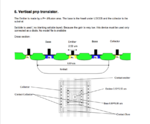
It's not a pmos, but a vertical pnp bipolar junction transistor (BJT) - even if the contacts all are at a horizontal level. In the center is the emitter, left and right in the N-well (sometimes around the emitter) the base contacts, outside of the N-well, left and right, or surrounding it, the p+ contacts of the P-Sub: the collector.

See here a cross-section and a topview of such a 0.35µm process vertical pnp BJT:
Vertical_pnp_transistor.png
 
thank you Erikl,

from the layout point of view it looks nice, but... how to connect the MOST in schematic to order to make a proper simulation? I think gate + the substrate + the source connect to the ground, and a signal put to the drain. Correct me if I am wrong.
 

I think your connection is right. However I don't know what is MOST in your schematic. I suspect it's the substrate connection, so you should connect it to GND.
 
... and a signal put to the drain. Correct me if I am wrong.

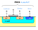
Drain corresponds to collector, base (or bulk tap) to base, and source to emitter - no gate at a BJT. So you should put the signal to the source.

See this image: not a symmetric example, unfortunately.
PMOS_or_PNP-BJT.png

In symmetric BJTs, the emitter is always in the center, s. the .
 
vadim888,

Are you to trying to connect a pmos as a vpnp but use a pmos model? I am not sure that will work.
 

vadim888,

Are you to trying to connect a pmos as a vpnp but use a pmos model? I am not sure that will work.

yes, but what can I do instead of this? I have to design a bandgap in CMOS technology, so no BJTs there...
 

... but what can I do instead of this? ... no BJTs there...

Just connect a pmos as shown in your image above (additionally connect the gate with the source). For N diodes use N such pmos transistors - each one connected as such a diode - in parallel. In schematic keep the 1 + N diodes.
 
hi,

you can see the complete bandgap reference and simulation tutorial here
 
Hi.

Why we use diode ? Or why we use bipolar transistor? Ok, we need CTAT, so diode is CTAT? But can we use something else?
Can we bipolar replace with MOSFET in design?
Anybody to explane me that logic, why diode?
 

People have made, and do make delta-VT references which
act similarly. However they are subject to more influences
(and less controlled ones) than the simple diode or substrate
BJT. The BJT gain, poor as it is in a "substrate PNP" device,
helps to linearize the diode I/logV curve (you want that to
be linear on both sides of both single and N-fold diode groups'
operating current density, across the temperature range).

PN diodes can be designed so that little or none of the
forward current involves the surface interface, where the
trap density and surface recombination velocity are quite
process- and stress-variable. The junction itself is as well
controlled as the implant dose & energy (which is a process
control point that is monitored). Surface quality effects,
especially ones which bother minority carrier devices but
only affect CMOS leakage a little bit, not so much.
 
Status
Not open for further replies.

Part and Inventory Search

Welcome to EDABoard.com

Sponsor

Back
Top