Continue to Site

Welcome to EDAboard.com

Welcome to our site! EDAboard.com is an international Electronics Discussion Forum focused on EDA software, circuits, schematics, books, theory, papers, asic, pld, 8051, DSP, Network, RF, Analog Design, PCB, Service Manuals... and a whole lot more! To participate you need to register. Registration is free. Click here to register now.

balun and impedance matching circuit know hows

Status
Not open for further replies.

robismyname

Full Member level 6
Full Member level 6
Joined
Jan 17, 2008
Messages
390
Helped
11
Reputation
22
Reaction score
9
Trophy points
1,298
Location
Central Florida
Visit site
Activity points
4,603
Im using the CC2540. It has differential outputs. I am planning to make a Balun to make the output single ended so that it can interface to Inverted F antenna (Zo = 50 ohms).

My question is can the Balun be used to not only convert from differential to single output but to match to inverted F. Or do I have to make a different circuit after the balance stage to do the matching to Inverted F 50ohms characteristic impedance?

It is confusing to me because if you look at the reference design that TI provides for the CC2540 it shows a whole bunch of discrete passive components between the CC2540 and the antenna and I cant distinguish between the Balun circuitry and the matching circuit circuitry.

https://www.ti.com/lit/ds/symlink/cc2540.pdf
 
Last edited:

Yes you can, it have a normal DC decoupling and a synthetic Lattice balun consisting of a LC and CL circuit. By adjusting L/C ratio of the balun is also impedance ratio adjusted. Keep phase shift constant +/- 90 degree.
In the TI example is also a low pass filter following the balun, that is needed for suppressing harmonics. In this circuit, if low pass filter is omitted will probably main signal power level drop, so better keep the filter. Filter values must also be adjusted if balun impedance ratio is changed. That filter can also be used as a part of correcting complex impedance mismatch.
You need a VNA to verify results and for minimal number of matching components must matching be done between two complex curves (balun and antenna).
For best result should not only antenna have a matching impedance at main frequency, it should also be reactive mismatched for spurious frequencies.
For this kind of a bit complicated impedance matching do I recommend my own software, AnTune which makes the job real easy.


Thank you for your prompt reply. Although your answer is excellent I still have a few questions.

I will use software to test/evaluate TI's reference design but I would like to build my own test board to corroborate TI's balun design as well. So my questions are in regards to testing TI's design with hardware not sw applications at thsi point in time.

Please clarify for me the following:

If i were to mesure with a VNA the cc2540's side of the balun will the balun be matched to or close to the 2540's Zo of 70+30j? and will the other side of the balun be matched to or close to the antenna Zo of 50?

If I were to fabricate my own pcb test board with the same amount of pads to support TI's reference design and then populate the pcb with the parts they suggest (perhaps not including the LPF initially) how would I connect the side of the balun that connects to the CC2540 to a VNA? And should I expect to see 2540's Zo of 70+30j on that side of the Balun?

Same for the Antenna side of the balun If I were to fabricate my own pcb test board with the same amount of pads to support TI's reference design and then populate the pcb with the parts they suggest how would I connect the side of the balun that connects to the Antenna to a VNA? And should I expect to see Antenna's Zo of 50 on that side of the Balun?

So picture if you will a test board that has all the parts TI referenced for the balun populated on the board. I then want to measure the characteristic impedance on the cc2540 side of the Balun. What impedance should I expect to see on the 2540's side of the Balun? and how would I hook this test board up on the 2540's side of the balun to the vna? since there are two ports on the baluns 2540 side.

Again picture if you will a test board that has all the parts TI referenced for the balun populated on the board. I then want to measure the characteristic impedance on the antenna side of the Balun. What impedance should I expect to see on the antenna side of the Balun? and how would I hook this test board up to the vna?

Also is there a concern about the L's and C's that TI selected not performing well in 2.4GHz frequency applications?
 
Last edited:

If i were to mesure with a VNA the cc2540's side of the balun will the balun be matched to or close to the 2540's Zo of 70+30j? and will the other side of the balun be matched to or close to the antenna Zo of 50?
The balun can't be impedance matched, it is a transfomer between two impedances. If both sides are known can a transformation ratio be calculated. Do not forget that also reactive part will be transformed.
how would I connect the side of the balun that connects to the CC2540 to a VNA?
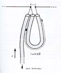
If your VNA have a balanced probe or if the VNA support differential measurements between two ports, use that. I do usually use a 1/2 lambda coaxial probe. It have a impedance ratio 1:4.
coax_balun.jpg
My homemade differential probe for 2.4 GHz. This kind of probe have a limited frequency range were readings can be assumed correct. It is good enough for my needs in 2.4 - 2.5 GHz span. It is not solid connected, it is just handheld for probing.
how would I connect the side of the balun that connects to the Antenna to a VNA?
Follow this link:Text and photos how to connect a measurement coaxial cable.
A balun can not correct both resistive and reactive part if different ratio for those both parameters are needed. That do the matching network take care of.
What impedance that will be measured is not only depending on what chip that have been selected, it also depends a lot of type of PCB and CU trace width & length, dual/singel side, ground stability, type of inductors... At 2.4 GHz can small variations in these factors result in very different readings.
TI recommend in several places in their web to exactly follow existing reference design (Gerber and component types/values) without questions, if you not can correctly measure and calculate your own values. There is a good reason. The type of questions in TI forum is much related to less good home-brew RF designs, resulting in poor performance.
TI also gives a bit different values for several CC25xx chip impedance, depending if it is for reference design or demoboard. These values where probably correct in each situation.
TX impedance for CC2540 is not the same as RX input impedance which not is he same as RX impedance for best SNR (which is rather frequency depending). Impedance resulting max output level differ from impedance resulting in best efficiency. It is several alternative impedances you have to play with.
When I design with these chips, are components values selected based on my own measurements. Data sheet impedance value is more a information in what range to expect the impedance. A bit same as with antennas, impedance for an typical antenna can be given as a general value, but is in reality very much depending on environment where it is placed.
 
  • Like
Reactions: FvM

    FvM

    Points: 2
    Helpful Answer Positive Rating
The balun can't be impedance matched, it is a transfomer between two impedances. If both sides are known can a transformation ratio be calculated. Do not forget that also reactive part will be transformed.

Ok thanks for the info. I think I have enough info to execute a plan. There is one thing I would like to clarify or rephrase from my previous question you tried to answer (in the above quote).

Earlier I asked "If i were to measure with a VNA the cc2540's side of the balun will the balun be matched to or close to the 2540's Zo of 70+30j? and will the other side of the balun be matched to or close to the antenna Zo of 50?"

My question was poorly written. What I was really trying to say was the following:

"There are two sides of this Balun. Differential side and Single ended side. Differential side is for the CC2540 connection. Single side is for antenna connection. If i were to measure with a VNA the differential side of the balun (not connected to the CC2540) what should I read with the VNA? Should it be in the range of the the CC2540's Zo of 70+30j? And also for the single ended side of the balun (when not connected to the antenna), if I were to measure with a VNA should I read something in the range of 50 ohms?

So basically picture in your mind a fabricated test pcb that uses TI's balun reference design. For clarity lets say the right side of the board is the differential connection. The left side of the board is for single ended connection. When I connect the differential side of my test pcb to the VNA I should measure a Zo around 70+30j at around 2.4GHz right? When I connect the single side of my test pcb to the VNA I should measure a Zo around 50 ohms at around 2.4GHz right?

If your VNA have a balanced probe or if the VNA support differential measurements between two ports, use that. I do usually use a 1/2 lambda coaxial probe. It have a impedance ratio 1:4.

So what you are saying is that I can measure the differential side of my test pcb in two ways:
1) using a VNA balanced probe if one is available
or
2) vna mode selected to support differential measurements between two ports

why use a 1/2 lambda coaxial probe? So your VNA does not support differential measurements between two ports? Did your 1/2 lambda come with your VNA? What is the significance of having a impedance ratio of 1:4? How is that beneficial?
 
Last edited:

70+30j at around 2.4GHz right?
Do not know how or trust these values, but assume that is what we have at output pins, and if PCB CU pattern is loss-less matched as 70 Ohm transmission line, you will measure 70 +xx Ohm were xx is 30j + phase delay.
When I connect the single side of my test pcb to the VNA I should measure a Zo around 50 ohms at around 2.4GHz right?
If you have a balun with 7:5 ratio, yes for the resistive part but reacktive part, which from beginning was +30j must also be included.
why use a 1/2 lambda coaxial probe?
Depends on your needs. This probe is cheap, simple, slim and resulting pins distance fits often well with actual measurement object.
So your VNA does not support differential measurements between two ports?
No.
Did your 1/2 lambda come with your VNA?
As I did wrote, is it a homemade probe. One among several similar homemade probing tools. Some done for a special measurement occasion and others for more general use.
What is the significance of having a impedance ratio of 1:4?
None. In general is measuring dynamic better if probe impedance is in same range as measurement object => More of resulting measurement will be centered at Smith chart.
 
Hi, Kafeman,

For the probe made by yourself, what is the length of the two stub?
 

    V

    Points: 2
    Helpful Answer Positive Rating
In theory 0.5 lambda but I did never measure.

1. A single coax, semi rigid, single center wire, which have 2-3 mm center tip visible is connected to VNA.
2. Adjust delay at VNA until the cable looks ideal open for a certain frequency. In my case 2.45 GHz.
3. Take a new coaxial cable part, in my case ¨50 mm long, solder braid against braid, tip against tip. Leave the other end of the 50 mm long coaxial cable unsoldered and open.
4. Check at VNA Smith chart while cutting down coaxial cable length a few mm each time. Goal is to almost be back at same Smith chart point, Open - 2 mm, because when stripping to get a few mm center pin also in this end of the coaxial cable will cost some electrical length.
5. Carefully bend this coaxial cable so it is possible to solder this 3:rd braid together with the other two.

The balun should now looks as in the photo above. Be careful when stripping for the tips, any knife cut will make center pin a lot weaker.
Verify that shorting between tips also shows a short at Smith chart and soldering a 200 Ohm resistor between tips shows 50 Ohm in VNA reasonable well.
Repeat that procedure when calibrating.
In AnTune, set system impedance at 200 Ohm which gives correct scaling also for the reactive part, and measuring a 200 Ohm resistor gives a dot in center of Smith chart.
Do not know if any VNA support this scaling internally or if it is possible to define it as a 200 Ohm calibration. A 3:rd alternative is to perform scaling manually for a saved S11 file.
Useable frequency bandwidth is about +/- 10%, depending on how big error that is acceptable.
 
In theory 0.5 lambda but I did never measure.

lambda/2 at 2.45Ghz is ≈ 2.4 inches. Is it better to make the coax stubs longer than this and then trim down a little at a time until you get to the open of the smith chart? I mean that is the goal right is to reach the open of the smith chart?

2. Adjust delay at VNA until the cable looks ideal open for a certain frequency. In my case 2.45 GHz.
are you talking about group delay or phase delay? What do you mean by adjust the delay? I thought the VNA measures/reads signal how can you adjust delay with vna? Can you clarify what you mean by this?

Verify that shorting between tips also shows a short at Smith chart and soldering a 200 Ohm resistor between tips shows 50 Ohm in VNA reasonable well.

Please confirm that for a 1:4 coax balun:
if the probe was built correctly a 200 ohm resistor at the probe leads will show 50 ohms at the vna and if i place the probe leads onto the differential side of my lattice balun (assumed to be matched for 70+30J) I should expect to see 17.5+7.5j at the vna? so the coaxial balun will transform both real an imaginary or just real?

Again thanks for the clarity in your feedback.
 

It's not been explicitely mentioned in the differential probe discussion, but I presume that you'll perform a SOL calibration at the differential side?

The main adavantage of the two port differential measurement, besides bandwidth is that it gives access to common mode impedances. To verify the performance of a LC balun, it's common mode S-parameters should be checked, too. It's e.g. interesting to know the common mode transmission of spurs and harmonics.

P.S.: I see, the first point has been answered clearly in post #8.
 

It's not been explicitely mentioned in the differential probe discussion, but I presume that you'll perform a SOL calibration at the differential side?
Yes that is correct. This type of calibration must be supported in VNA or manually defined as a specific cal.kit. Using setting for another cal.kit can result in reactive poor calibration.
It's e.g. interesting to know the common mode transmission of spurs and harmonics.
Agree, but if you find that kind of information interesting from design view, do you probably also know enough to understand limitation of this type of probe design and probing limitations in common.

Actually is RF-probing a mine field. A few possible things to avoid when probing:
Solving problems related to harmonics in a 2.45 GHz chip with "almost differential" output can be real evil as harmonic leakage can be in any direction from chip. Trying to track the problem with this type of probing can make anyone real confused.
I think actual chip, CC2540, have a hidden area below the chip that must be grounded to avoid harmonics of many flavors. Not possible to inspect optically or probing.
It is not unusual to find inductors in RF path that can be close or above SRF at 5 GHz or above => probing can result in almost any readings.
This balun is a load that affects the circuits.
This balun is a DC shortcut => Not all chips survive a measurement.

Yes, I have seen the smoke.
 
Last edited:
  • Like
Reactions: FvM

    FvM

    Points: 2
    Helpful Answer Positive Rating
In the TI example is also a low pass filter following the balun, that is needed for suppressing harmonics. In this circuit, if low pass filter is omitted will probably main signal power level drop, so better keep the filter. AnTune which makes the job real easy.

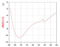
Ran analysis using Agilent's ADS and found out that the lattice balun with the LPF using the values suggested by TI tells me that my return lost is -6db at 2.4Ghz, VSWR of 3:1. Return lost is -10.8, VSWR of 1.8:1 @ 850MHz. See figure 1


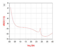
Ran analysis again without the LPF (just the Balun) my return lost is -11db at 2.4Ghz, VSWR of 3:1. Return lost is -11dB, VSWR of 1.8:1. See figure 2


LPF network makes RL worse at 2.4GHz. Or is the worsening of RL due to something else? How do I improve this?
 

I can confirm that a simulation with lumped components according to the datasheet values if far-off the said impedance. I guess the secret is in the parasitic circuit impedances, particularly trace inductances, not surprizing with 1-3 nH range of lumped inductors. You should try with a simulation of the complete reference design geometry.
 

Status
Not open for further replies.

Part and Inventory Search

Welcome to EDABoard.com

Sponsor

Back
Top