Continue to Site

Welcome to EDAboard.com

Welcome to our site! EDAboard.com is an international Electronics Discussion Forum focused on EDA software, circuits, schematics, books, theory, papers, asic, pld, 8051, DSP, Network, RF, Analog Design, PCB, Service Manuals... and a whole lot more! To participate you need to register. Registration is free. Click here to register now.

avoiding to use pads as vias.

Status
Not open for further replies.

black_flowers

Junior Member level 2
Joined
Sep 23, 2007
Messages
23
Helped
0
Reputation
0
Reaction score
0
Trophy points
1,281
Activity points
1,437
does somebody know how to avoid altium to use pads as vias? I know i can define a via keepout rule for each area i want to apply this rule but i'm wondering if there is a rule for avoiding it on the whole board.

thanks!:wink:
 

If you can apply rule to area what's the problem in applying it ti the board.
Second i didnt got you r question of using pads as vias could please be more clear.
 

Do I guess right, that you want to block connections to the top side pads of through plated component padstacks? It hasn't to do with via keepout rules. You have to modify the padstack or add blocking areas to the component definition.
 
and how can i do that? This is the pad properties, i don't know what should i modify to get the pins non connected on the bottom layer.

Imageshack - pinvk.jpg
 

Why do you not want to use a PTH pad to transfer a track from one side to the other?

because there are some connectors that has only the top layer visible because the bottom is covered by the body connector. And pdip microcontrollers are placed on connectors too, in order to unplug them for reprograming them.
 

Sorry, but that still does not explain it ?

Are you saying that you want your tracks to only exit a PTH pin on the top side only and not the bottom? (or vis versa)

If so, is this not achieved by manually routing them while having the layer set as the one to route on?

Your comments about connector bodies and PDIP micro's do not make sense, what have connector bodies got to do with the tracks?
 

i cannot explain myself quite well in english, excuse me.

as you say, the layers are wrong, where i said top i mean bottom an viceversa.

yes, this can be done with manually routing (but i want to use autoroute)

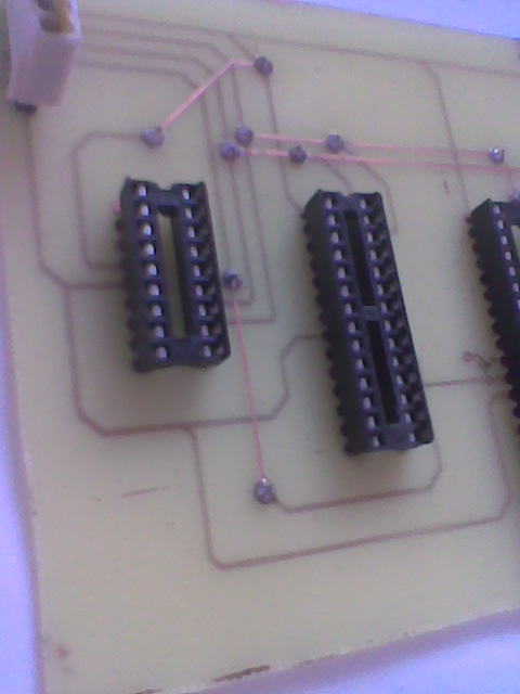
what i mean when i said that bodie component doesn't allow me to access pads is this:
47_1283682121.jpg


as you can see in the image i cannot access pads on the bottom layer. I would like to know how to change pads properties for avoinding routing on bottom layer, because i could use autorouting and i could route the boards faster.

thanks!
 

So your doing a single sided prototype board?

If it is like the one shown in the photo then why use autorouting?
It would take longer to setup autorouting than it would to do the manual routing in the first place.

If you want to autoroute it, can you not just tell it to autoroute on the one layer?

I think that in cadstar you are able to add an attribute to the pad to tell it what side to route from, can you do this in your package?

Another option would be to use turned pin sockets, for those you are able to get to the pins to solder them on the top.
 

the circuit i'm making is not like the circuito on the photo. Nor the circuit on the photo nor the circuit i'm making are one sided, they are routed in both sides top and bottom. And in my opinion is easyer to make the rules than route board manually. Finally i did it placing keepout over pads i don't want to be routed.

thanks.
 

Status
Not open for further replies.

Part and Inventory Search

Welcome to EDABoard.com

Sponsor

Back
Top