Continue to Site
Follow along with the video below to see how to install our site as a web app on your home screen.
Note: This feature may not be available in some browsers.
hi,can u send me a pcb design and source code,
i want to make it in my final year project
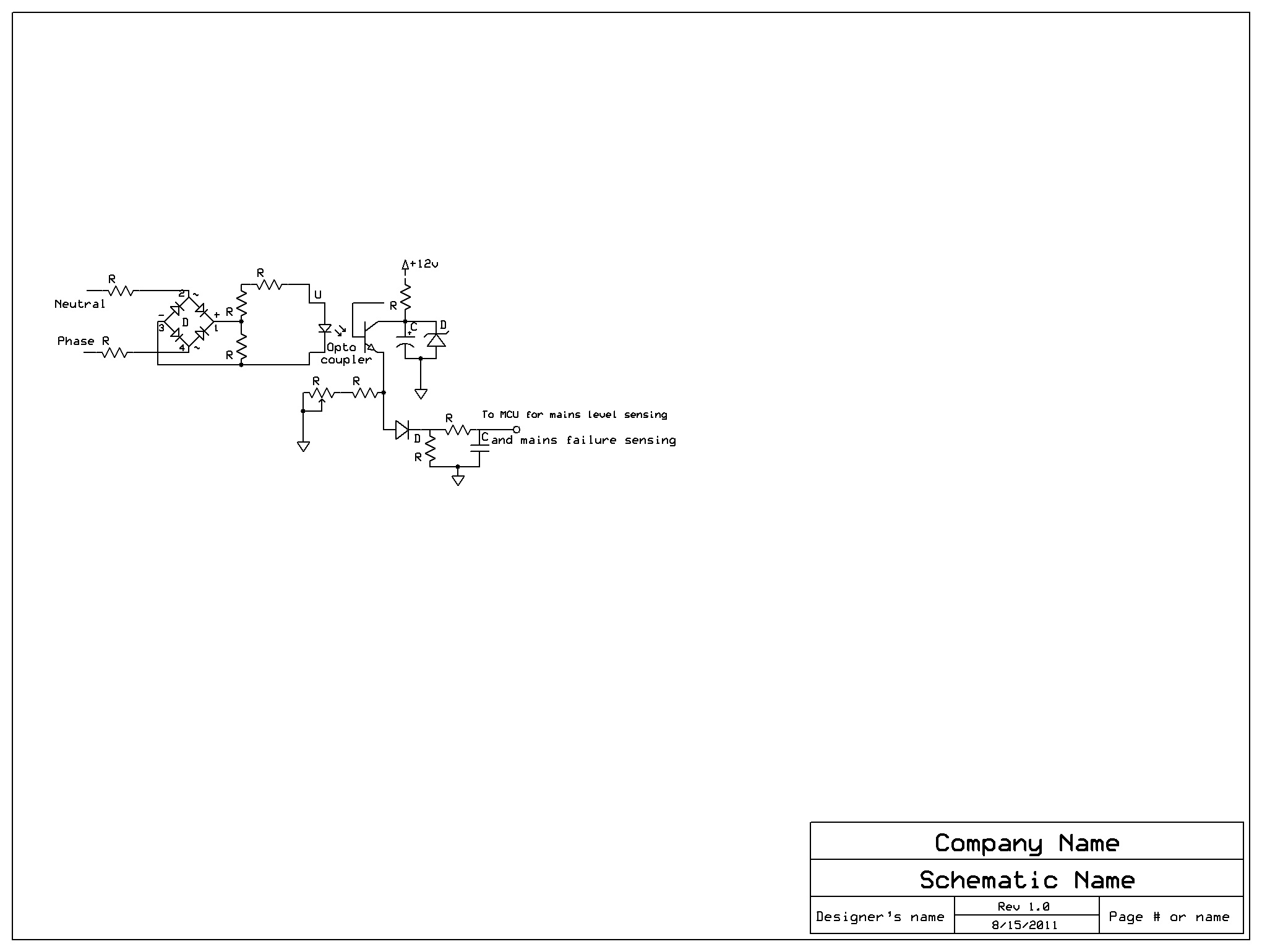
For PCB design see post number #53 and #79.hi,can u send me a pcb design and source code,
i want to make it in my final year project
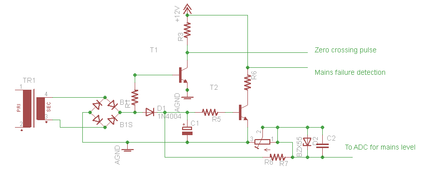
I suppose you need a capacitor at the output of the bridge. to smoothen the wave.
Hello there guys,
I have a doubt. This inverter uses what kind of transformer? HF transformer or the 50Hz normal transformer?