Continue to Site
Follow along with the video below to see how to install our site as a web app on your home screen.
Note: This feature may not be available in some browsers.
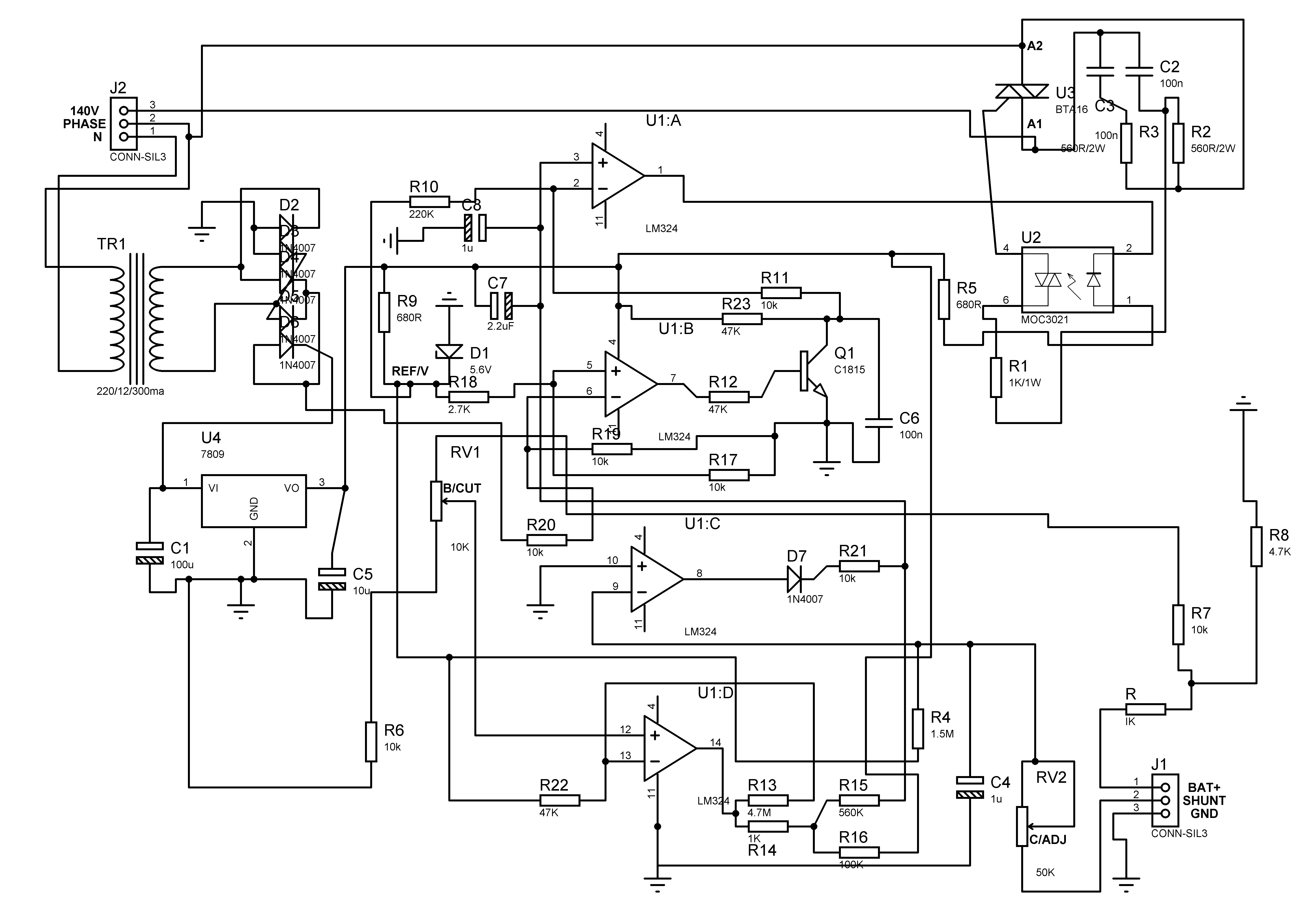
Sahu,try this schematic,you can made it at vero board.this schematic consist of LM324,BTA16,MOC3021.
Its difficult,fault is due to charging system(anti parl SCR) in your inverter.my inv kit like above charing controlling .my problem i can't any change my inv. i want modification only o\l scening circuitry & C.T. (turn ratio) only .
Hi TahmidHi pnjbr,
Your observations are correct except that the RC does not work as filter but as snubber.
Yes, battery can not be touched. That's because of no galvanic isolation as I opted not to have another small transformer in the circuit and I find this is no problem as usually the battery is kept within a "container" where you can not touch the battery or the terminals.
I can see the pcb layout but wondering how you can pick up so much details about the schematic from within that pcb.
that is very good of you, i just thought maybe the schematic is posted somewhere else.
My Regards
Hi pnjbtr,
I already uploaded the PCB design. You just need to resize that. Do you mean physically send one PCB?
@ babaloa,
Hi. I will upload a schematic soon, but school just started and I'm so busy, I'm not getting time.
Tahmid.
Hi,
What is your location? Where are you from?
---------- Post added at 19:41 ---------- Previous post was at 19:40 ----------
@babalola,
I'll try and help with your project. What should we start with?
I think i should try with pcb layout.but to reduce size i need file in original format. because i saw some copper traces are without whole(looking like for SMD component).Especially where you contact leds header to ic pins and all vary able resistors(trimpots)except multy turn(feed back) have no holes.