kapil_vlsi1
Member level 2
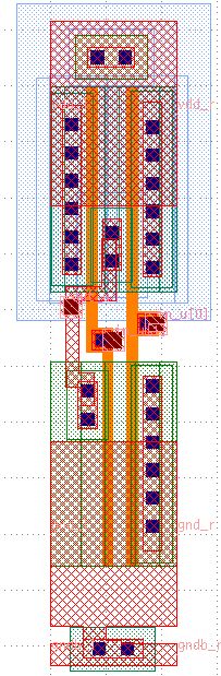
nand gate area
Hi all,
Kindly let me know what could be the are in Micrometer for 180 nm process. Please advise. Expecting ur reply.
Regards
Hi all,
Kindly let me know what could be the are in Micrometer for 180 nm process. Please advise. Expecting ur reply.
Regards