Continue to Site

Welcome to EDAboard.com

Welcome to our site! EDAboard.com is an international Electronics Discussion Forum focused on EDA software, circuits, schematics, books, theory, papers, asic, pld, 8051, DSP, Network, RF, Analog Design, PCB, Service Manuals... and a whole lot more! To participate you need to register. Registration is free. Click here to register now.

Arbitrary pcb shape design using Altium Designer

Status
Not open for further replies.

rizwan183

Member level 4
Member level 4
Joined
Feb 15, 2013
Messages
70
Helped
6
Reputation
12
Reaction score
6
Trophy points
1,288
Location
Pakistan
Visit site
Activity points
1,817
i am looking to design a PCB antenna using Altium Designer. But i could not figure out how to design an arbitrary shape such as circle in Altium. Any suggestions?
 

you can draw any shape in altium. example you can use "Place>Full circle" command for circle. You can make Arc, straight line, etc., Make sure you have selected a net from the object property menu(By double clicking the object). Another way, you can import 2D outline from anyother software in DXF format and pour "polygon" inside the layout.
Draw any closed loop 2D outline (Example : Full circle), select the entire object & follow this. Tool>Polygon Pours>Define from selected objects
 

Attachments

  • Polygon pour.PNG
    Polygon pour.PNG
    26.2 KB · Views: 185
First Of All Thanx for your response. For me first method somehow worked to design something like attached though not look like a proper way. And as for as DXF format i tried a single 2D circle export it using HFSS options. But this didn't worked. I don'nt know why. If you have some practice material related this Do share the links. And One More question how can i define my board shape to be round? Thank You
 

Attachments

  • Capture.JPG
    Capture.JPG
    15.1 KB · Views: 195

Draw a circle with the desired diameter, select it, then click "Design" => "Board Shape" => "Define from selected objects". Alternatively, draw the shape you like in your favorite CAD software and then import it into Altium as a STEP file. You can then use the same technique to define the board shape from the STEP contour.
 
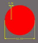
Actually my issue is to draw multiple void circles ( areas without copper) of radius 0.49 mm inside a bigger copper circle as shown in my second post. Poly gone pour commands does not work properly in here. Issue is precision. If I use polygon pour command the results would be inaccurate because of High frequency. Can I do this using Altium? If so, how is this possible? The issue with dxf file import error is dimensions of the document too large and as for as the step file does not supported by Altium. Kindly help me on this.
 

As I understand if you need only the circular copper tracks, you can make it with simple circle command with very good precision. If you need any other odd shape, its always better to use a DXF file format. If possible give me a required shape information in drawing format.

Regards
Udhay
 

Dear Udhay, I have attached the a rough Design.in this white circles corresponds to copper free areas with a radius of 0.49 mm and the bigger circle is 32 mm. Black area represents copper. if we define a circle and then use a "polygon pour=>Define for selected objects" then it give a circle having copper free area in the mid and between the circle and and 2D circle obtined from Polygon Pour as dimensions (0.49mm) is comparable to the line width.
 

Attachments

  • New Bitmap Image.gif
    New Bitmap Image.gif
    6.8 KB · Views: 173

It's actually not my choice. with that much variation Response changes drastically because of high frequency.
 

Making 0.49 dia is very critical. Very much possible with drill hole. Check this...
 

Attachments

  • Capture.PNG
    Capture.PNG
    13.3 KB · Views: 167
How you take these exact measures. Is it using polygon pour command and consider the null effect of the command before hand.And Thanks a lot buddy for you Help I am able to use .DXF format.
 

Status
Not open for further replies.

Part and Inventory Search

Welcome to EDABoard.com

Sponsor

Back
Top