Continue to Site

Welcome to EDAboard.com

Welcome to our site! EDAboard.com is an international Electronics Discussion Forum focused on EDA software, circuits, schematics, books, theory, papers, asic, pld, 8051, DSP, Network, RF, Analog Design, PCB, Service Manuals... and a whole lot more! To participate you need to register. Registration is free. Click here to register now.

Antenna Violation Fix

Status
Not open for further replies.

S.Nikhil

Member level 1
Joined
Oct 9, 2007
Messages
34
Helped
18
Reputation
36
Reaction score
17
Trophy points
1,288
Activity points
1,553
Hi,

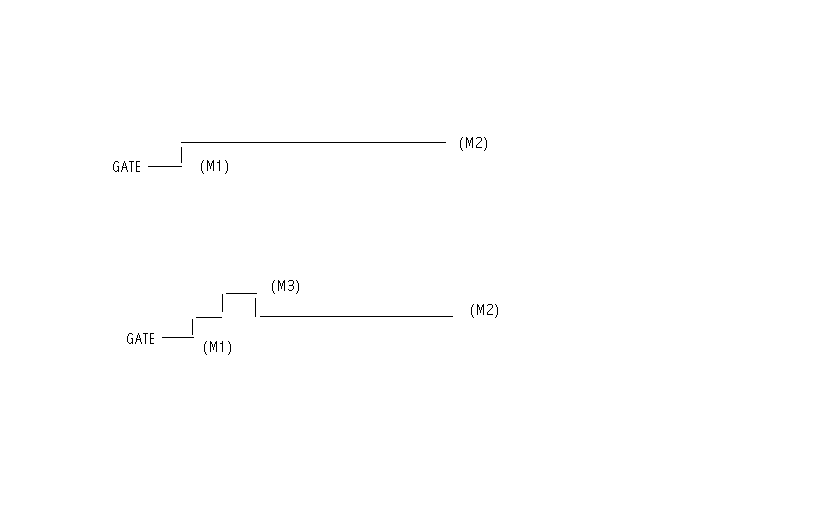
I know that layer hopping can be used as a way to fix antenna violation, but does this mean that by only moving from lower metal layer to top metal layer antenna violations can be fixed or can it be even done by moving from top metal layers to bottom metal layers.


Thx

S.Nikhil
 

It can be done either way. The antenna phenomenon has to do with the length of one stripe of wire during the manufacturing process. When you change layers, you move to a different wire and only one of the wires will be there during the plasma processes. And since you have to come back to the layer of the driving port anyway, it doesn't matter. There is just a limit to the length of a net that's only connected to an input port during the manufacturing process.
I think you can also fix this by switching to antenna resistant cells (with diodes for example), cells with large gate oxides.
 

The key thing to understand about antenna probems is that you are worried about a high voltage zapping through the thin gate oxide of a CMOS transistor.

Long wires exposed to the plasma etching used during IC manufacturing can accumulate a considerable amount of charge (like an antenna picking up radio energy from the air). If this wire is already connected to a transistor gate then the voltage can discharge through the oxide.

What 'layer hopping' does is to make a short break near the end of the wire so that it does not connect down to the gate pin, and then replaces the missing piece by a short bridge on a *higher* layer. The trick is that the long wire now can accumulate its charge without any risk to the gate because there is no connection to it yet (remember, the higher layers are manufactured later than the lower layers!). When it's the turn of the short bridging section to be manufactured it is too short to act as an antenna and the long wire is safely buried under a layer of insulating oxide.

Below I've tried to draw a cross section of a long wire on metal-2 before and after 'layer hopping' to metal-3


------------------------------------------------- (M2)
|
Gate---- (M1)


------ (M3)
| |
--- --------------------------------------- (M2)
|
Gate---- (M1)
 

Sorry, the picture did'nt come out the way I expected. I have fixed it below:

[/img]
 

Status
Not open for further replies.

Part and Inventory Search

Welcome to EDABoard.com

Sponsor

Back
Top