Continue to Site

Welcome to EDAboard.com

Welcome to our site! EDAboard.com is an international Electronics Discussion Forum focused on EDA software, circuits, schematics, books, theory, papers, asic, pld, 8051, DSP, Network, RF, Analog Design, PCB, Service Manuals... and a whole lot more! To participate you need to register. Registration is free. Click here to register now.

A High PSRR Bandgap problem

Status
Not open for further replies.

alias0823

Junior Member level 1
Joined
Mar 9, 2004
Messages
17
Helped
1
Reputation
2
Reaction score
1
Trophy points
1,283
Location
Taiwan
Activity points
112
high psrr bandgap

Dear all

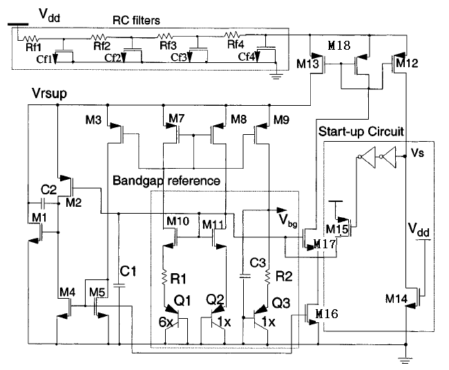
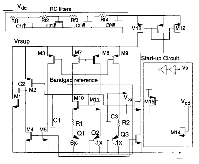
I have some question about this bandgap, which is reference from "A Supply-Noise-Insensitive CMOS PLL With a Voltage Regulator Using DC-DC Capacitive Convertor" by Chang-Hyeon Lee,..

In this paper, no detail description about how it works, and only mention RC filter to filte supply noise, and simple start up.

my question is: What is the role of M1, M2, and M13? Can somebody help me to solve it?

56_1171541704.gif
 

high psrr bandgap reference

it looks like it is helping to bring the vdd supply to vrsup in case the gate of M10/M11 is too low (won't start up).
 

self biasing psrr

I think M13 is a common source for all PMOS branch.
However, I don't understand the role of M1 and M2.
 

a low supply voltage high psrr

The role of M1 and M2 is to improve the PSRR.
 

nagaraj a low supply voltage high psrr

yes, I agree with bw9601's idea
It can improve the PSRR
M1 and M2 has a negtive feedback.

when it is stable ,Vrsup is a stable voltage.
 

This is self-biased bandgap structure (M13). M13 is providing all the bias currents for the bandgap. Thus, even without M1 and M2, it will work with pretty decent PSRR. However, it may not be very safe design without M2 (M1 is just giving more gain.). If M13 doesn't provide the exact amount of bias current for the bandgap, this circuit will collapse but with M2, this will be prevented.
 

"The RC passive filter comprised of the Rf1-Rf4 and C1-C4 filter attenuate supply noise at frequencies larger than the response capability of the bandgap reference circuit."

I want to know how to determine the parameters Rf1-Rf4 and C1-C4?
How to simulate this RC passive filter?
Which parameters should be cared?
How much should the -3dB frequency of the RC passive filter?

Thanks.
 

wjlzhx said:
yes, I agree with bw9601's idea
It can improve the PSRR
M1 and M2 has a negtive feedback.

when it is stable ,Vrsup is a stable voltage.

I strongly agree with your opinion, but the DC voltage on gate of M2 would influence the reject performance; to let the M2 always working in active region when in normal operation at different corner situation is a challenge.
 

Thanks all

I need to modify the circuit more clear

86_1172740933.gif


Added after 23 minutes:

As I know, M1,M2,M3,M4, and M5 are error amplifier to sense the difference of Vds7 and Vds8, and feedback to Vrsup

But I have another question, what is the role of M17?
 

alias0823 said:
As I know, M1,M2,M3,M4, and M5 are error amplifier to sense the difference of Vds7 and Vds8, and feedback to Vrsup

But I have another question, what is the role of M17?

Yes, you are right, M1-M5 force Vds7=vds8 by modulating Vrsup through current shunt action of M1, realizing better current matching between M7 & M8.

M17 works as cascode transistor to reduce bias current variation with Vdd in branch M16-M18.
 

M1 M2 ,i think, provides (with the help of Capacitor) a load which improves PSRR.
M17 as i see is switching ON the current mirror with the help of startup ckt..
M13 (1st ckt.) necessarily provides current to the ckt.
 

any papers on this structure?

Added after 12 minutes:

Khong-Meng Tham and Krishnaswamy Nagaraj "A Low Supply Voltage High PSRR Voltage Reference in CMOS Process" IEEE JOURNAL OF SOLID-STATE CIRCUITS, VOL. 30, NO. 5, MAY 1995
 

I think in this design to have good PSRR, the Vrsup need to be regulated. That mean the M13 transistor must supply more current than it required by the bandgap circuit (M7, M8, M9 branches). M3, M5 and M4 is the bias circuit for M2. The M2 and M1 is used to regulated the Vrsup by sinking the excess current that is not required by the bandgap block. M1 is the gain stage for the regulated Vrsup loop. So it needs to be compensated by C2 using miller compensation.

So, it is important that the M13 transistor supplies more than bandgap block and the bias circuit so that M1 can be used to provided the control to regulated the Vrsup.
 

the role of the m13 is to improve psrr, because it is a high resistor node. the role of the m1 and the m2 is to bias the right current.
 

Status
Not open for further replies.

Similar threads

Part and Inventory Search

Welcome to EDABoard.com

Sponsor

Back
Top