analog_chip
Full Member level 1

- Joined
- Oct 9, 2011
- Messages
- 99
- Helped
- 1
- Reputation
- 2
- Reaction score
- 1
- Trophy points
- 1,288
- Activity points
- 1,994
Hi,
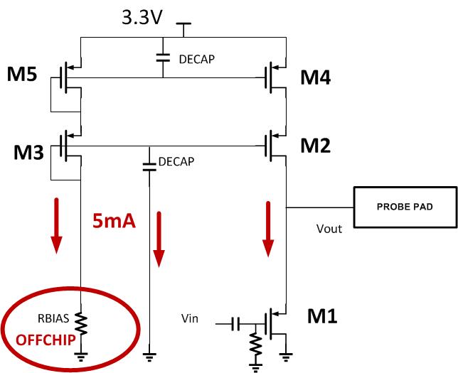
I want to design a 50 ohm buffer in frequency range 10MHz-40MHz which will be followed by wafer probes and then instruments. The baseband output of a receiver will be buffered.
I am planning for PMOS source follower with
a) current source load
b) resistive load
PMOS for low flicker noise. Which one is better a) or b).
Any other suggestion? I have no power limit. I need low noise.