Welcome to our site! EDAboard.com is an international Electronics Discussion Forum focused on EDA software, circuits, schematics, books, theory, papers, asic, pld, 8051, DSP, Network, RF, Analog Design, PCB, Service Manuals... and a whole lot more! To participate you need to register. Registration is free. Click here to register now.
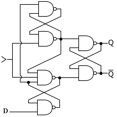
The FlipFlop is usually described as "positive-edge-triggered". You find the same gate level diagram for TTL IC 7474 (with additional nPRE and nCLR inputs).
Please notice, that all usual edge-triggered circuits, e.g. CMOS transfer gate designs are level sensitive at the transistor level and don't involve any dynamical circuits e.g. with capacitors. Edge sensitive means, that the input state is sampled and transferred to the output during the clock edge, at no time there's a direct input to output connection as in a transparent latch.
Correct edge sensitive behaviour can be only guaranteed if the specified maximum CLK risetime is kept.
There's a maximum rise time specification in most logic datasheets. For slow clock edges, correct operation isn't guaranteed. With some digital devices, clock inputs may have an internal schmitt-trigger circuit to overcome the problem.
This site uses cookies to help personalise content, tailor your experience and to keep you logged in if you register.
By continuing to use this site, you are consenting to our use of cookies.