Continue to Site

Welcome to EDAboard.com

Welcome to our site! EDAboard.com is an international Electronics Discussion Forum focused on EDA software, circuits, schematics, books, theory, papers, asic, pld, 8051, DSP, Network, RF, Analog Design, PCB, Service Manuals... and a whole lot more! To participate you need to register. Registration is free. Click here to register now.

Microphone Amplifier Design Problem

Status
Not open for further replies.

jegues

Member level 3
Joined
May 29, 2011
Messages
58
Helped
0
Reputation
0
Reaction score
0
Trophy points
1,286
Activity points
1,915
We are attempting to design a amplifier for a microphone. The end goal is to amplify what is being said through the microphone specified below through a set of speakers or headphones.

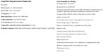
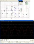
See figure attached for the design parameters as well as the parts list we are given.

Note: The output current is limited to a maximum of 20mA.

I'm a little flustered with all the requirements of this design in addition to the limited parts list. I'm having trouble figuring out how I should start my design or even what direction to move in.

What kind of stages I should be considering with the components I'm provided? Should I focus on one aspect of the design at first (i.e. gain requirement) and sort out the others later on? If so, which design aspect is crucial to achieve before attempting to establish other design parameters?

Can someone give me a push in the right direction so I can get this design started?

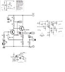
I went and asked my professor for a good point to start and he had recommened that I start by considering the specific input and outputs we're given, and make an attempt at designing the amplification stage of the amplifier. I'm a little confused about what I'm supposed to deduce about my inputs/outputs given the datasheet of the microphone, can someone clarify?

He mentioned to me that in this stage I need to achieve the required gain as well as the bandwidth, and mentioned that if I could not achieve both in one stage that I should simply use 2 amplification stages to achieve the required bandwidth and gain.

I've attached the datasheet specific to the microphone we are provided.

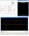
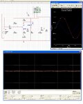
I will be posting whatever design/results/thoughts I come up with for more feedback/improvement.

Thanks again!
 

Attachments

  • AMPROJ.jpg
    AMPROJ.jpg
    67.1 KB · Views: 88
  • HM-31066-P88%20REV%20A%20%282.1%29.pdf
    277.8 KB · Views: 91

I'd suggest you start by choosing a relatively simple 9V circuit of the many 2-transistor circuits available by searching for "microphone amp" from G00gle images. To this you add a simple complementary class AB output stage. Then take the feedback for the 23dB gain from the output.
 
  • Like
Reactions: jegues

    jegues

    Points: 2
    Helpful Answer Positive Rating
I'd suggest you start by choosing a relatively simple 9V circuit of the many 2-transistor circuits available by searching for "microphone amp" from G00gle images. To this you add a simple complementary class AB output stage. Then take the feedback for the 23dB gain from the output.

I did just as you had recommended and google'd around for some images. I've attached what I've found to this thread.

To be perfectly blunt I don't fully understand all of the underlying details of each component and it's specific purpose related to a given schematic, but I do have a fairly broad understanding of circuits and amplifiers configurations such as common emitter, common base in addition to things such as coupling capacitors etc...

Do any of the schematics in the image I've posted seem to be useful for the task I have to complete? If so, which ones and why?

Also, as I was googling around I see lots of talk about Dynamic Amplifiers and Preamplifiers, what is the distinction between the two and which pertains to my specific design?

It looks like we're moving in the right direction!

Thanks again!

EDIT: It seems to be as though the schematic in the top left corner of the image I've posted is the most straightforward and basic. Will a schematic like this be enough to satisfy the design requirements I am required to meet? If not, can I tweak it to do so? Or should I pursue a different design?
 

Attachments

  • VariousMicAmps.JPG
    VariousMicAmps.JPG
    122.1 KB · Views: 94
Last edited:

Here's a design I tried and simulated in multisim.

Note: I assumed 100mV peak input at 1kHz, I'm not sure whether this is actually what my microphone will provide.

The results seem pretty promising if I'm not making mistakes anywhere.

See figure attached.

If we look at the values we obtain on the scope we can quickly calculate the gain in dB's.

\[\text{Voltage gain} = \frac{13.768mV}{999.337uV} = 13.777134 \frac{V}{V}\]

Now put this into dB's,

\[20log(13.777134) = 22.783178 dB\]

Which almost ideal for the required 23+/-3dB gain we desire.

Am I making any mistakes here or are my results indeed valid?

EDIT: I tried my amplifier again attaching the nominal load of 60 ohms and the output and my gain gets completely destroyed. (See 2nd figure attached)

Is there a way to fix this? Or did I do something wrong?
 

Attachments

  • MicrophoneSim1.JPG
    MicrophoneSim1.JPG
    322.5 KB · Views: 74
  • MicrophoneSim2.JPG
    MicrophoneSim2.JPG
    317.4 KB · Views: 84
Last edited:

Hi, jumping in here.

Is this a project you're supposed to design only, or to build as well? Because it's a lot to handle before one has gone through the earlier steps leading up to it.

You state the instructor recommends doing the project in stages. It suggests the way to start is with a simple 1-transistor amplifier. Class A operation (simpler than B or AB). Capacitor inline with the speaker/headphone.

(Sidebar)... After I was not able to 'get it' by reading books about basic electronics, I still remember the fun on the day I decided to hook up 5 or 6 components with jumper clippers, spoke into a microphone, and heard my own voice come out of a speaker. I didn't realize it would be that easy.

The simple 1-transistor amplifier may not perform to spec. However by optimizing the basic setup you will identify concepts of operation. You'll spot certain things that cause better or worse performance.

You'll notice what adjustments yield the greatest gain for your microphone. Also what is a good range of operation for the transistor so you get greatest voltage swing while at the same time not to waste current..

Then you can move up to satisfying the other specs. Two transistors (if needed). AB operation. The 20mA maximum current spec. Flat frequency response. Etc.

This is a useful project which might be adaptable to things such as creating your own mp3 player system, etc.

You may have found a schematic (top left corner) which meets the design specs. Using it unmodified may be the fastest path to completing the project. You'll learn a lot either route you take.

Keep in mind however that the instructor may ask you to explain current paths, or tell why you put a component here rather than there, or how you chose a certain value, or what causes a node to be at a certain voltage, etc.
 

You may have found a schematic (top left corner) which meets the design specs. Using it unmodified may be the fastest path to completing the project. You'll learn a lot either route you take.


Can you help me understand why I'm losing my gain when I attach the nominal load at the output? How can I prevent this from happening?
 

Your load needs several mA going through it in order to meet specifications.

Your load is powered by the output transistor turning mostly on, then mostly off.

This results in reciprocating current flow back and forth through the load. In from the output transistor, then back through resistor R6.

R6 is 10k ohms.

The transistor may be in the correct operating range. It may turn on sufficiently to power your load.

However when the transistor is almost turned off, your load has only that 10K resistor to conduct through. It's impossible for more than a mA to flow during that half of the cycle.

Hence the loss of gain.

It would help if you were to try various values for R6.

I just finished trying multiple values for R6 on the same circuit I've posted with no significant change in the gain I've observed based on the values from the scope.

Am I doing something wrong? Is there any value in particular that would significantly repair my gain?

I'm still a little lost on this one.
 

Your latest change was to install a load of comparatively low resistance, among components which have comparatively high resistance.

It caused a big change in circuit behavior.

It helps if you adjust components gradually. That way you can spot a bad trend and try something else.

Changing one component often makes it necessary for you to adjust other components as well.

Anyway, just to make this easy...

Change the load to 1k ohm. This will alter behavior but not so drastically that you can't spot what direction the output is going. Change R6 in such a direction as to bring things back to proper operation. Or change the bias current, etc.

Another tip... The 100nF capacitor is too small to pass audio frequencies to a low impedance load.

The problem I'm experiencing with my gain when the load is attached is clearly a loading issue correct?

If this is the case, couldn't I rectify the problem by simply inserting a buffer stage inbetween the coupling capacitor and the load?

Would a simple emitter follower do the trick?
 

The problem I'm experiencing with my gain when the load is attached is clearly a loading issue correct?

If this is the case, couldn't I rectify the problem by simply inserting a buffer stage inbetween the coupling capacitor and the load?

Would a simple emitter follower do the trick?

No, for such a low load impedance I'd suggest a class AB output buffer, s. the foll. PDF: View attachment class-AB-buffer_sch.pdf

Some notes:
  • You probably must change R6 in order to get ≈VDD/2 = 4.5V at the junction of R10 & R11
  • The pre-driver stage (Q2..R6) will have lower gain than before, and the output buffer stage (QN2/QP2) has a gain < 1
  • That is why you'll have to change the feedback resistor R5 to restore the necessary gain
Good luck! erikl
 
  • Like
Reactions: jegues

    jegues

    Points: 2
    Helpful Answer Positive Rating
No, for such a low load impedance I'd suggest a class AB output buffer, s. the foll. PDF: View attachment 63708

Some notes:
  • You probably must change R6 in order to get ≈VDD/2 = 4.5V at the junction of R10 & R11
  • The pre-driver stage (Q2..R6) will have lower gain than before, and the output buffer stage (QN2/QP2) has a gain < 1
  • That is why you'll have to change the feedback resistor R5 to restore the necessary gain
Good luck! erikl

Thanks erikl!

I'm going to implement the buffer you've shown in the diagram post my results.

I will try to make the adjustments you've mentioned in order to obtain 4.5V at the junction of R10 & R11, and tweak R5 such that the gain is restored.

Check back for my progress, I might need more help!
 

See figure attached for my updated circuit and simulation.

I was able to restore the gain back to ~23dB by tweaking the value of R5, but I wasn't able to set R6 such that the voltage at the junction of R10 and R11 is ~4.5V.

Is it crucial that it sits at exactly 4.5V?

As the meter shows in the figure, I currently have it sitting at 3.5V. I tried ranging R6 from a 10 ohms to 10Mohms but I would only see slight increases or decreases in the voltage at the junction, and it would often result in ruining my gain.

Is what I have so far reasonable, or is there other improvements that I should make?
 

Attachments

  • OrigCAB.JPG
    OrigCAB.JPG
    299.5 KB · Views: 81

All this is progress. A push-pull amplifier is the solution for you to get a lot of decibels while limiting current draw to 20mA

However are you allowed to use 4 transistors according to the design rules?

To get the meter to read V/2, I think you'll have to make Q2's average impedance match the resistance in the corresponding position on the totem pole. This is R6.

To achieve this there's a chance you'll need to adjust a value or two in an earlier stage.

Continue to experiment. You should not just get the circuit operating, but have an idea why the correct component values work correctly, and why other values didn't work.

Yesterday you were flustered. Since then with help from this board you've made progress toward the assingment. The help is given cheerfully and with the aim to encourage. However you need to be able to show the instructor you can do it on your own, just in case he singles you out in front of the class as an exemplary student.
:^)

I agree with everything you've mentioned above. This is indeed a learning process for me and I'm still continuing to learn as I progress through the assignment.

You mention that in order to obtain a voltage of 4.5V at the junction of R10 & R11 I must match the average impeadance of Q2 with R6.

What is the average impeadance of a transistor defined as?

After I know that, hopefully I can make an attempt at adjusting some of the values in earlier stages in such a way that this is possible.

Thanks again!
 

... I wasn't able to set R6 such that the voltage at the junction of R10 and R11 is ~4.5V.
Is it crucial that it sits at exactly 4.5V?
Actually for your task it is not, as you need only a max. of 500mVss output voltage.
However, in order to achieve the highest possible output voltage (≈8Vss) this would be crucial. You could achieve this by increasing Q1's base voltage, e.g. by increasing R2 .

I tried ranging R6 from a 10 ohms to 10Mohms ...
This has no effect on gain or output quiescent voltage. These resistors are only useful against output short circuit protection, and to reduce the quiescent current through the output transistors Q3 & Q4. Reasonable values are between 0 and 10Ω , with this latter value you probably push the quiescent current through the driver stage below 1mA (battery lifetime!).

Is what I have so far reasonable
Yes, absolutely!

... is there other improvements that I should make?
I'd suggest to separate the power supply of the electret mic (0.5mA) and the first preamplifier stage (Q1) by an appropriate RC combination from the 9V battery power supply. This is apt to decrease interferences from the output stage, see e.g. the right-most circuit of your circuit collection from your post #3.

Moreover I'd suggest to replace the output stage transistors (Q3 & Q4) by the available and more powerful PN2907 & PN2222 devices.
 
Last edited:
  • Like
Reactions: jegues

    jegues

    Points: 2
    Helpful Answer Positive Rating
To get the meter to read V/2, I think you'll have to make Q2's average impedance match the resistance in the corresponding position on the totem pole. This is R6.
I think, there's a misunderstanding of the circuit operation. The output voltage is set by DC feedback and the ratio of R1/R2, that can be adjusted accordingly. R6 in constrast sets the bias current of the output stage. The crossover distortion suggests, that it may need to be increased, there's however a problem of output transistor's limited power rating.

P.S.: I reviewed the specification, which requires only 0.5 Vpp output. In so far exact output bias voltage isn't an issue. It's also obvious, that the output will first clip due to limited current sink capabilty rather than output saturation. Of course the cicruit can be optimzed in different directions, but after adjusting the gain (and possibly increasing C1), it meets the specification.

P.P.S.: The idea of matching Q2 to R6 is complete nonsense. If you want to change the output bias voltage, adjust R1 or R2. The C1 value of 100n is also O.K.. Lower -3 dB corner is about 50 Hz now.
 
Last edited:
  • Like
Reactions: jegues

    jegues

    Points: 2
    Helpful Answer Positive Rating
... I must match the average impeadance of Q2 with R6.
What is the average impeadance of a transistor defined as?

The quiescent output impedance of a common emitter (in this case) transistor with its collector load resistor RL (ro || 1/gm || RL).

You can affect this by tweaking its collector current (via the base voltage), or -- essentially -- by the value of the collector load resistor (R4 in your case).
 
  • Like
Reactions: jegues

    jegues

    Points: 2
    Helpful Answer Positive Rating
You mention that in order to obtain a voltage of 4.5V at the junction of R10 & R11 I must match the average impeadance of Q2 with R6.

What is the average impeadance of a transistor defined as?

Its resistance should range above and below R6 so that its average is the same as R6.

I say this because your amplifier appears as though it will operate symmetrically after those components. Unless I'm missing something.

So if R6 is 10k, then Q2 should vary between 5000 ohms and 15000 ohms. Or between 1000 and 19000. I can't be sure how large the real voltage swing is. Because you would not be able to directly measure Q2's resistance moment to moment, but you would judge by the voltage swing.

So to vary the operating range of Q2, you would tweak the values of R1 through R4. Maybe R6 as well. Only slight changes are needed at this point.
 
Last edited:

Q2 is more a controlled current source than an impedance or resistance. It's average current is ruled by the DC feedback path over Q1. As said, you need to adjust R1/R2 to modify the output bias voltage. By setting R2 to 180k, you get almost perfect mid voltage.
 
  • Like
Reactions: jegues

    jegues

    Points: 2
    Helpful Answer Positive Rating
Status
Not open for further replies.

Similar threads

Part and Inventory Search

Welcome to EDABoard.com

Sponsor

Back
Top