Continue to Site

Welcome to EDAboard.com

Welcome to our site! EDAboard.com is an international Electronics Discussion Forum focused on EDA software, circuits, schematics, books, theory, papers, asic, pld, 8051, DSP, Network, RF, Analog Design, PCB, Service Manuals... and a whole lot more! To participate you need to register. Registration is free. Click here to register now.

PCB design 450 MHz LVDS trace routing

Status
Not open for further replies.

engr_joni_ee

Advanced Member level 3
Joined
Nov 3, 2018
Messages
718
Helped
2
Reputation
4
Reaction score
4
Trophy points
18
Activity points
5,940
Hi,

I am going to design with 8 layers having LVDS 450 MHz traces. I am just wondering about the Stack-up scheme. How about the following arrangement of layers.

Layer 1 : Routing
Layer 2 : Routing/Ground
Layer 3 : Ground
Layer 4 : Power
Layer 5 : Power
Layer 6 : Routing/Ground
Layer 7: Ground
Layer 8: Routing

Is it necessary to have one ground plane between two power planes or not ? Any comments on the above layer arrangement ?
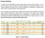
 

Hi you can try this stack up you know LVDS traces must be 80 ohm

Stackup.png
 

Hi, Thanks for suggestion. Kindly send me in good quality. I am not able to read small numbers.
 

Nominal LVDS differential impedance is actually 100 ohms, but compromises are possible.
 

Agree, most are 90-100, PCIe goes down to 85, but cant find any at 80... so I would aim for a 100 or get the spec for the interface you are laying out and READ IT.
 

100 ohms differential is the same as two 50-ohm-to-
common-mode-point impedances, and no conductance
to the ground plane (provided that balance is good and
skew is nil). Maybe 50-ohm high frequency trace design
is a "freebie" utility in the PCB tool that does well enough
if you terminate it differentially (not to the plane)?
 

LVDS standards are based on 100 ohms differential impedance and if LVDS receivers are equipped with internal termination (some FPGAs, receiver ICs), it can be expected to show 100 ohms.

It can make nevertheless sense to use a lower differential impedance, e.g. if the pairs are routed on inner layers with low substrate height, termination resistors have to be adjusted respectively.
 

100 ohms differential is the same as two 50-ohm-to-
common-mode-point impedances, and no conductance
to the ground plane (provided that balance is good and
skew is nil). Maybe 50-ohm high frequency trace design
is a "freebie" utility in the PCB tool that does well enough
if you terminate it differentially (not to the plane)?

100r diff is not alway equal to two 50r SE lines, depends on PCB geometry. Skew is the most important factor according to Howard Johnson and a couple of others.
 

100r diff is not alway equal to two 50r SE lines, depends on PCB geometry.
50r SE means zero coupling (infinite separation) of differential lines, that's rather impractical. A typical common mode impedance of the differential pair is in the 30 to 40 r range, respectively 60 to 80 r SE impedance. Low separation and high SE impedance means smallest room requirement.
 

Status
Not open for further replies.

Part and Inventory Search

Welcome to EDABoard.com

Sponsor

Back
Top