venkates2218
Full Member level 6

Code:
#define XTAL_FREQ 20MHZ
#include <xc.h>
#include "delay.h"
// CONFIG1H
#pragma config OSC = HS // Oscillator Selection bits (HS oscillator)
#pragma config FCMEN = OFF // Fail-Safe Clock Monitor Enable bit (Fail-Safe Clock Monitor disabled)
#pragma config IESO = OFF // Internal/External Oscillator Switchover bit (Oscillator Switchover mode disabled)
// CONFIG2L
#pragma config PWRT = ON // Power-up Timer Enable bit (PWRT disabled)
#pragma config BOREN = OFF // Brown-out Reset Enable bits (Brown-out Reset disabled in hardware and software)
#pragma config BORV = 3 // Brown Out Reset Voltage bits (Minimum setting)
// CONFIG2H
#pragma config WDT = OFF // Watchdog Timer Enable bit (WDT disabled (control is placed on the SWDTEN bit))
#pragma config WDTPS = 32768 // Watchdog Timer Postscale Select bits (1:32768)
// CONFIG3H
#pragma config CCP2MX = PORTC // CCP2 MUX bit (CCP2 input/output is multiplexed with RC1)
#pragma config PBADEN = OFF // PORTB A/D Enable bit (PORTB<4:0> pins are configured as digital I/O on Reset)
#pragma config LPT1OSC = OFF // Low-Power Timer1 Oscillator Enable bit (Timer1 configured for higher power operation)
#pragma config MCLRE = ON // MCLR Pin Enable bit (MCLR pin enabled; RE3 input pin disabled)
// CONFIG4L
#pragma config STVREN = OFF // Stack Full/Underflow Reset Enable bit (Stack full/underflow will cause Reset)
#pragma config LVP = OFF // Single-Supply ICSP Enable bit (Single-Supply ICSP disabled)
#pragma config XINST = OFF // Extended Instruction Set Enable bit (Instruction set extension and Indexed Addressing mode disabled (Legacy mode))
// CONFIG5L
#pragma config CP0 = OFF // Code Protection bit (Block 0 (000800-001FFFh) not code-protected)
#pragma config CP1 = OFF // Code Protection bit (Block 1 (002000-003FFFh) not code-protected)
#pragma config CP2 = OFF // Code Protection bit (Block 2 (004000-005FFFh) not code-protected)
#pragma config CP3 = OFF // Code Protection bit (Block 3 (006000-007FFFh) not code-protected)
// CONFIG5H
#pragma config CPB = OFF // Boot Block Code Protection bit (Boot block (000000-0007FFh) not code-protected)
#pragma config CPD = OFF // Data EEPROM Code Protection bit (Data EEPROM code-protected)
// CONFIG6L
#pragma config WRT0 = OFF // Write Protection bit (Block 0 (000800-001FFFh) not write-protected)
#pragma config WRT1 = OFF // Write Protection bit (Block 1 (002000-003FFFh) not write-protected)
#pragma config WRT2 = OFF // Write Protection bit (Block 2 (004000-005FFFh) not write-protected)
#pragma config WRT3 = OFF // Write Protection bit (Block 3 (006000-007FFFh) not write-protected)
// CONFIG6H
#pragma config WRTC = OFF // Configuration Register Write Protection bit (Configuration registers (300000-3000FFh) not write-protected)
#pragma config WRTB = OFF // Boot Block Write Protection bit (Boot block (000000-0007FFh) not write-protected)
#pragma config WRTD = OFF // Data EEPROM Write Protection bit (Data EEPROM not write-protected)
// CONFIG7L
#pragma config EBTR0 = OFF // Table Read Protection bit (Block 0 (000800-001FFFh) not protected from table reads executed in other blocks)
#pragma config EBTR1 = OFF // Table Read Protection bit (Block 1 (002000-003FFFh) not protected from table reads executed in other blocks)
#pragma config EBTR2 = OFF // Table Read Protection bit (Block 2 (004000-005FFFh) not protected from table reads executed in other blocks)
#pragma config EBTR3 = OFF // Table Read Protection bit (Block 3 (006000-007FFFh) not protected from table reads executed in other blocks)
// CONFIG7H
#pragma config EBTRB = OFF // Boot Block Table Read Protection bit (Boot block (000000-0007FFh) not protected from table reads executed in other blocks)
#define data LATDbits.LATD1 /*Output control*/
#define clock LATDbits.LATD0 /*Output control*/
int check_1[] = {0, 0, 0, 0, 0, 0, 0, 1};
int check_2[] = {0, 0, 0, 0, 0, 0, 1, 1};
int check_3[] = {0, 0, 0, 0, 0, 1, 1, 1};
void port_setting(void) {
TRISA = 0b00000000;
PORTA = 0b00000000;
CMCON = 0X07;
TRISB = 0b00000000;
PORTB = 0b00000000;
TRISC = 0b00000000;
PORTC = 000000000;
TRISD = 0b00000000;
PORTD = 0b00000000;
TRISE = 0X00;
PORTE = 0X00;
}
void main(void) {
port_setting();
while (1) {
for (int y = 0; y <= 8; y++) {
clock = 1;
data = check_1[y];
DelayMs(100);
clock = 0;
}
while (1) {
}
}
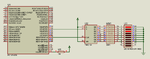
}This is the circuit and code used to interface 74HC164N with PIC controller.
I tried to switch ON every output pins in 74HC164N one by one.
By using the above code,1,2,3 outputs are working in shift register.
If I used like
Code:
int check_4[] = {0, 0, 0, 0, 1, 1, 1, 1};
int check[] = {1, 1, 1, 1, 1, 1, 1, 1};
to turn on 4th and 5th pin in shift register means not working.
How to solve this issue.