Continue to Site

Welcome to EDAboard.com

Welcome to our site! EDAboard.com is an international Electronics Discussion Forum focused on EDA software, circuits, schematics, books, theory, papers, asic, pld, 8051, DSP, Network, RF, Analog Design, PCB, Service Manuals... and a whole lot more! To participate you need to register. Registration is free. Click here to register now.

Help needed! - Design of class-C RF PA using ADS

Status
Not open for further replies.

Simo.Da

Junior Member level 2
Joined
Jul 15, 2018
Messages
23
Helped
0
Reputation
0
Reaction score
0
Trophy points
1
Activity points
295
Hello everyone,

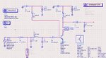
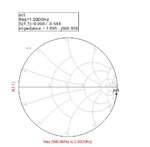
I have managed to design a Class-A amplifier at 1 GHz (see attached) using ADS
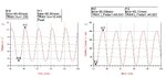
Now, I have to drive it harder to move it from class-A to class-C (From linear mode to non-linear)
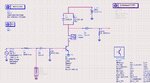
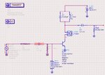
I did some modifications on the circuit but I am not quite sure about the correct steps!
I have to investigate into how the resonant circuit affects the output power, and then the efficiency as a function of a conduction angle and so on.

Is there anybody can help with the right starting off steps please?
N.B: I am still new to an RF design world, so please make it simple as much as you can

Your help is much appreciated
 

Attachments

  • Class-A PA.JPG
    Class-A PA.JPG
    127.8 KB · Views: 459
  • Class-A PA output.JPG
    Class-A PA output.JPG
    90.5 KB · Views: 303
  • Class-C PA.JPG
    Class-C PA.JPG
    119.7 KB · Views: 314

There are many errors in your schematic.Test set-up is also wrong..
Model parameters are also inconsistent..BF=987, VAF=380 ??? They are out of spec of a RF transistor which will work at 1GHz.
100mH//25uF ?? What is that ??
 
* Do a calculation for impedance of C6 at 1GHz to make sure it will pass 1 GHz.

* I think R3 should be several k ohms. With its value 50 ohms I think it will divert all of the bias to ground. The transistor will not turn on.

* Your LC tank looks as though the L & C values are high, creating a slow resonant frequency. Did you obtain these values by using the standard formula for resonant frequency?

* And does the tank create an impedance which is compatible with your expected Ampere levels?
 
Thank you BigBoss for your comment
Those model parameters are for "BFP740F" transistor which's dealing with RF till 45GHz
The 100mH//25uF supposed to resonate at 1GHz, but I'm not sure if those calculations are right, thereforeI am asking for a help
 

* Do a calculation for impedance of C6 at 1GHz to make sure it will pass 1 GHz
The impeadance presented at the base of the transistor is 7.695-j598.838, please correct my if I am wrong (screenshots attached)

* I think R3 should be several k ohms. With its value 50 ohms I think it will divert all of the bias to ground. The transistor will not turn on
You this could be done by experiment!?

* Your LC tank looks as though the L & C values are high, creating a slow resonant frequency. Did you obtain these values by using the standard formula for resonant frequency?
I have modified the value depends on f=1/2pi*sqrL.C to 25pF/1nH

* And does the tank create an impedance which is compatible with your expected Ampere levels?
Sorry I don't understand this exacty
 

Attachments

  • Zin.JPG
    Zin.JPG
    80.9 KB · Views: 228
  • Impedance.JPG
    Impedance.JPG
    33 KB · Views: 196
Last edited:

I post a typical C-Class Amplifier here, you can continue by inspiring ,,
c_class.pngc_class_current.png

There is no matching,no optimization, no Load Pull etc.It's just an example and principal schematic.Pay attention to biasing circuit.This one may be different manner but in principle, VBE must be negative in order to maintain C-Class operation.
Note: BFP740F is not very suitable transistor for C-Class amplifier.It's very convenient A-Class Low Noise Amplifier.
 
* And does the tank create an impedance which is compatible with your expected Ampere levels?

To explain my question:
It has to do with the L:C ratio. You can make two LC tanks with an identical resonant frequency, however one develops large voltage swings, while the other develops small voltage swings.

Suppose you have low current levels in your circuit... then you want a high L:C ratio.

If you wish to have heavy current flowing in your circuit, then you want a low L:C ratio.

This parameter has a part in your stated objective, to explore resonance and output power.
 
There are so many design steps in designing class C power amplifier.

Why your load is too big ?

First you have to find your optimum load approximate value.

Pout = 1/2 * VDD * I1 (I1 is load current 1st harmonic or fundamental tone)

lets say

Pout = 1W and VDD=5 (assuming your transistor can handle this voltage)
then I1 = 0.4

then your load should be

Ropt = VDD/I1 = 5/0.4 = 12.5 not 252 !

you can calculate Imax to see what should be your size for your max input voltage

I1 = (Imax/2*pi) * ((a-sina)/(1-cos(a/2))
for class C 0 < a < pi

This is just a begining to give you an idea

- you should have loadpull setup to see what is exact real load (load should be complex not only R for getting more power)
-While doing loadpull you may use a LC tank at the output to trap your harmonics. It can be simple LC tuned at 1GHZ.
- you should do loadpull while having matching at input.

There so many setups involved in PA design and it is hard to explain them here.
 
Thanks BradtheRad,
In order to find the optimal value for tank circuit component, I have to calculate the Q factor first which can be calculated as Q=Fc/BW
Next, the source and load resistance are combined to determine the total parallel resistance of the circuit using Rp= Zs.Zl/Zs+Zl
After that the parallel reactance could be determined using Xp=Rp/Q
Finally, by substituting in L=Xp/w and C=1/w.Xp we can get the L and C value
The problem is in determining the source and load impedances as I thought they could be calculated using the input and output conjugate (as you can see in the attached screenshot) and I'm really confused!
Could you please advise?
Thanks Zs and Zl.JPG

- - - Updated - - -

Thanks Ata_sa16 for you easy and nice explanation

I have started with a simple steps I read them from Power Amplifiers book (photos attached) as below:

1. Vce(max)=2Vcc /In datasheet it is 13V so I assumed it 11V to stay a little bit away from it/ so Vcc=5.5
2. Ic(max)=45 mA /depending on the transistor's datasheet I also assume to be 40mA as a safety margin/
3. I am confused between Ip and I1 current?
4. Do I need to assume any value for Theta to be between 0 and 180?
5.
you can calculate Imax to see what should be your size for your max input voltage
Does Imax different from the Ic(max)?

Sorry for the load of questions :-?

- - - Updated - - -

Thanks Ata_sa16 for you easy and nice explanation

I have started with a simple steps I read them from Power Amplifiers book (photos attached) as below:

1. Vce(max)=2Vcc /In datasheet it is 13V so I assumed it 11V to stay a little bit away from it/ so Vcc=5.5
2. Ic(max)=45 mA /depending on the transistor's datasheet I also assume to be 40mA as a safety margin/
3. I am confused between Ip and I1 current?
4. Do I need to assume any value for Theta to be between 0 and 180?
39994532_298292610975948_1528763123333332992_n.jpg
39929254_226852104648774_6829644680980856832_n.jpg
39960988_1988719871178966_3931510700802834432_n.jpg
 

The problem is in determining the source and load impedances as I thought they could be calculated using the input and output conjugate

The L & C values create a certain amount of impedance between your power supply and load. As a resonating LC tank, it will generate voltage swings of its own.

Your schematic has a load of 50 ohms, power supply 5.5 V. This calculates as 100 mA (in round figures) going through your output stage. It implies your inductor and capacitor values should each be able to pass 100 mA at your design frequency.

A very large inductor passes miniscule current at 1 GHz.
But a very small inductor requires large current to generate much voltage swing.

Obviously your inductor needs to be some middle value.
Same principle applies to your capacitor. Small C passes small current. Large C generates smaller voltage swing.

Below are formulae for reactive impedance. To find tentative values, solve for L & C so they produce 50 ohms impedance at 1 GHz. As you test and experiment with your circuit you will gravitate toward optimum values.

XL = 2 Pi f L

XC = 1/ ( 2 Pi f C )

I call the 'tentative' because accurate calculations require further steps, which take into account the phase changes.
 
1. Vce(max)=2Vcc /In datasheet it is 13V so I assumed it 11V to stay a little bit away from it/ so Vcc=5.5

good

2. Ic(max)=45 mA /depending on the transistor's datasheet I also assume to be 40mA as a safety margin/

So I1=Imax/2 then Pout = 55 mW

3. I am confused between Ip and I1 current?

It is complicated. Which book is this ?
read this book:

https://d1.amobbs.com/bbs_upload782111/files_45/ourdev_672470C259C6.pdf


4. Do I need to assume any value for Theta to be between 0 and 180?

yes


5.
you can calculate Imax to see what should be your size for your max input voltage
Does Imax different from the Ic(max)?

same

Sorry for the load of questions


No problem. you should be aware of this: PA design is harder than other RF blocks, specially simulations.
You need a lot of time and patience.
 
It is complicated. Which book is this ?
I am reading Modern Communication Circuits (2nd edition) - Jack R.Smith

Thanks for that, but I haven't found an example of designing Class C PA

I have chosen theta=90, so I got the below values (please let me know if there's any concern about these values)
I1=20 mA
Ropt=275 Ohms
Po=55 mW
Ip=40 mA (Does the peak value shouldn't exceed Ic(max)?)
Icc= 12.73 mA
Pcc= 70.03 mW
Pdis=15.03 mW
Efficiency= 78.5%

If you can see the attached screenshots, I have disabled the tank circuit to get the right output current
Here I got two questions:
1. What does specify the RF input amplitude? Is it by experiment until I get the maximum output power? Here I have set it to 0.947 V
2. I did understand that the tank circuit will work as a BPF, so it's gonna resonate at 1 GHz and reject any other harmonics. Does that lead to reconstruct the output current signal to be sinusoidal (without clipping)?
Optimal calculations.JPG
Optimal calculations output.JPG
 

W.Dabbas..

You make very serious mistakes in your C-Class Power Amplifier design..
-You made short circuit the LC tank circuit but the Ouput is short circuited directly to the GND.The amplifier won't work..
-You drive the amplifier with a sinusoidal Voltage Source without any source impedance, this is wrong.You should use a P_1Tone with 50 Ohm source impedance and you should also design a Input Matching Circuit for the amplifier
-Output should also be matched to wanted Impedance.You have to use either Load Pull technique or roughly speaking Load Line method.Output Impedances of the Power Amplifiers are pretty small.
-How you have measured the Output Power ?? There is no AC voltage across the Load.

You'd better read Grebennikov's RF Power Amplifier Design textbook.You have so many leaks about the Power Amplifiers.

I agree with all. All mistakes you have are very basic ones. I told you read some books before simulation.

Grebennikov's RF Power Amplifier Design, is better for nonlinear power amplifiers such as class E and F and it is not a basic book. It has an advanced explanation language.
As I told try Steve Cripps power amplifier design.
 

1. What does specify the RF input amplitude? Is it by experiment until I get the maximum output power? Here I have set it to 0.947 V

It is common to use a pullup resistor, in order to lift the transistor bias to 0.5 or 0.6 V. (Make it a variable resistor. Or use a potentiometer to provide any volt level from 0 to supply V.) Then it is feasible to reduce amplitude of your source signal.

Consider that you may need to install a resistor inline with the power supply. Between 10 and 100 ohms. Without it, the response tends to rise to supply V.

It is also common to install a parallel RC in the emitter leg. This allows DC operation to a degree, while the AC portion is amplified to a greater degree.

Class C operation has non-linear response, and so this suggests it may involve clipping.
 

Status
Not open for further replies.

Part and Inventory Search

Welcome to EDABoard.com

Sponsor

Back
Top