Continue to Site

Welcome to EDAboard.com

Welcome to our site! EDAboard.com is an international Electronics Discussion Forum focused on EDA software, circuits, schematics, books, theory, papers, asic, pld, 8051, DSP, Network, RF, Analog Design, PCB, Service Manuals... and a whole lot more! To participate you need to register. Registration is free. Click here to register now.

Help ADS Document for MMIC PA Design

pusparaga

Full Member level 4
Joined
Oct 19, 2013
Messages
197
Helped
4
Reputation
8
Reaction score
4
Trophy points
1,298
Activity points
2,988
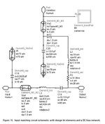
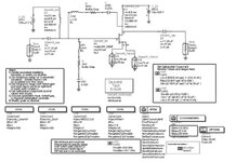
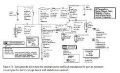
Like ADS CookBook, is there any help document available for Power Amplifier(PA) Design using MMIC Technology. In ADS CookBook, good example has given to desIgn PA at 1 GHz using Microwave Integrated Circuit (MIC).
Like ADS CookBook, help document available for design at any band PA design using MMIC technology. If anybody has help document, can you share.
 
Discrete OR MMIC OR RFIC, no matter Technology/Process you've been using, the Main Principles of Designing of an Power Amplifier are always same.
There are some different tricks or methods but they are essentially same.


I have attached MMIC ADS design document and Screen related to MMIC design of Amplifier. It looks similar to Microwave Integrated Circuit (MIC) design implementation. But in MIC Amplifier design, lumped values of resistance , capacitors and inductors are separated by using MLIN with larger width and length. After completing this, we are generating Gerber file and send it to Fabrication.
In MMIC Design, are we growing resistors, inductors and capacitors on the monolithic layer. What is the major difference between MIC and MMIC?
In MMIC design, are we using design kit values of L, C and R values. To separate these L,C and R , we are small using MLIN with small um width and length. Is it right, later we are generating Gerber file for layout.
 

Attachments

  • MMIC_CKT.pdf
    63.6 KB · Views: 63
  • Input matching circuit schematic, with design kit elements and a DC bias network.jpg
    Input matching circuit schematic, with design kit elements and a DC bias network.jpg
    96.2 KB · Views: 47
  • MMIC_Lumped_Ckt_Amplifier.jpg
    MMIC_Lumped_Ckt_Amplifier.jpg
    208.5 KB · Views: 43
  • MMIC_Lumped_Ckt_Amplifier_1.jpg
    MMIC_Lumped_Ckt_Amplifier_1.jpg
    151.8 KB · Views: 45
  • MMIC_Schematic_Ckt.jpg
    MMIC_Schematic_Ckt.jpg
    80.8 KB · Views: 46
  • The interstage matching network, including design kit elements and DC bias inductors.jpg
    The interstage matching network, including design kit elements and DC bias inductors.jpg
    127.5 KB · Views: 43
  • 5988-9637EN_2_MMIC_ADS_Design.pdf
    4.2 MB · Views: 61

LaTeX Commands Quick-Menu:

Part and Inventory Search

Welcome to EDABoard.com

Sponsor

Back
Top