Continue to Site

Welcome to EDAboard.com

Welcome to our site! EDAboard.com is an international Electronics Discussion Forum focused on EDA software, circuits, schematics, books, theory, papers, asic, pld, 8051, DSP, Network, RF, Analog Design, PCB, Service Manuals... and a whole lot more! To participate you need to register. Registration is free. Click here to register now.

Problem of lateral diffusion on SILVACO TCAD

Status
Not open for further replies.

yogesh5683

Newbie level 2
Joined
Dec 2, 2014
Messages
2
Helped
0
Reputation
0
Reaction score
0
Trophy points
1
Activity points
30
Hi everyone,
I am new on silvoco TCAD,i am designing a device on it of 32nm fgmos but the problem here is "lateral diffusion" and the junction is not finding properly,
the command i used for it is
implant arsenic dose=1e15 energy=10
pleaase suggest me proper command that i can use to implant n type material by reducing lateral diffusion for 32nm fgmos.

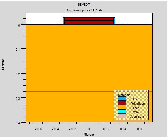
the output seeems like this
 

Attachments

  • FGMOS.JPG
    FGMOS.JPG
    32.9 KB · Views: 130

You are not showing the dopants in the attached picture, just the structure.
Post your code.
 

go athena

Code PHP - [expand]
1
2
3
4
5
6
7
8
9
10
11
12
13
14
15
16
17
18
19
20
21
22
23
24
25
26
27
28
29
30
31
32
33
34
35
36
37
38
39
40
41
42
43
44
45
46
47
48
49
50
51
52
53
54
55
56
57
58
59
60
61
62
63
64
65
66
67
68
69
70
71
72
73
74
75
76
77
78
79
80
81
82
83
84
85
86
87
88
89
90
91
92
93
94
95
96
97
98
99
100
101
102
103
104
105
106
107
108
109
110
#TITLE: EEPROM cell formation example
#
 
line x loc=0.0  spac=0.005 
line x loc=0.032  spac=0.00125
line x loc=0.045  spac=0.0025
line x loc=0.075  spac=0.01
#
line y loc=0.00 spac=0.0005
line y loc=0.015  spac=0.0015
line y loc=0.1  spac=0.0125
 
#
init c.boron=3e16 orientation=100 space.mult=1
 
#
method compress fermi
diffuse time=1 temp=950 dryo2 
#
etch oxide thick=0.001
extract name="tunnelox" thickness oxide mat.occno=1 x.val=0
#
implant boron dose=1e12 energy=25 
#
deposit poly thick=.0125 div=4
#
implant phos dose=6e14 energy=30 
#
diffuse time=0.5 temp=950 dryo2 
etch oxide thick=0.002
extract name="oxy" thickness oxide mat.occno=1 x.val=0
#
deposit nitride thick=0.001 div=1
#
deposit oxide thick=0.0005 div=1
#
deposit poly thick=.0125 div=4 c.phos=8e19
# 
etch poly    right p1.x=0.03
# 
etch oxide   right p1.x=0.03
# 
etch nitride right p1.x=0.03
#
etch oxide   right p1.x=0.03
#
etch poly    right p1.x=0.03
#
etch oxide   right p1.x=0.03
#
relax y.min=.015 dir.y=f
#
implant arsenic dose=1e15 energy=10 
#
diff time=50 temp=950
deposit oxide thick=.0015 div=2


#
structure mirror left
#
etch oxide left  p1.x=-0.04
etch oxide right p1.x=0.04
 
deposit alum thick=0.0025 div=1
#
etch alum start x=0.045 y=-10.
etch alum cont x=0.045 y=10.
etch alum cont x=-0.045 y=10.
etch alum done x=-0.045 y=-10.
#
# define electrode names
electrode name=fgate x=0 y=-0.005
electrode name=cgate x=0 y=-0.02
electrode name=source x=-0.075
electrode name=drain x=0.075 
electrode name=substrate backside
# save the structure
#structure outfile=eprmex01_0.str
#
#tonyplot  eprmex01_0.str -set eprmex01_0.set
 
# Switch to Devedit for remeshing...
go devedit
 
 
# Set Meshing Parameters
#
base.mesh height=0.02 width=0.02
#
# Make sure impurity gradiants have enough detail. (i.e. no triangle
# spans more than 1 (sensitivity=1) power of 10)
imp.refine imp="NetDoping" sensitivity=1
imp.refine min.spacing=0.001
#
# Make sure channel has enough triangles.
constr.mesh depth=0.0125 under.material="PolySilicon" max.height=0.0025 \
        max.width=0.0025
constr.mesh depth=0.0025 under.material="PolySilicon" max.height=0.00075
#
# Make sure contacts have enough connection points.
constr.mesh depth=0.0025 under.material="Aluminum" max.width=0.05
 
# Create a mesh, using the parameters set above.
mesh mode=meshbuild
 
# save structure
struct outfile=eprmex01_1.str
tonyplot  eprmex01_1.str -set eprmex01_1.set


quit
 
Last edited by a moderator:

Status
Not open for further replies.

Part and Inventory Search

Welcome to EDABoard.com

Sponsor

Back
Top