Continue to Site

Welcome to EDAboard.com

Welcome to our site! EDAboard.com is an international Electronics Discussion Forum focused on EDA software, circuits, schematics, books, theory, papers, asic, pld, 8051, DSP, Network, RF, Analog Design, PCB, Service Manuals... and a whole lot more! To participate you need to register. Registration is free. Click here to register now.

What does this circuit do?

Status
Not open for further replies.

znoopie

Newbie level 3
Joined
Aug 23, 2012
Messages
3
Helped
0
Reputation
0
Reaction score
0
Trophy points
1,281
Activity points
1,321
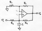
It is given that the input node vi has low impedance and the output node vo has high impedance. The question is "What does this circuit do?".

Assuming that op-amp's gain is very large, I computed the transfer function and got vo/vi = 2/(s*R2*C), which is an integrator or a low-pass filter.

However, I'm still skeptical about the information on the input/output impedance. I thought it would affect the circuit's function in some way. Help or comments are appreciated.

Thanks in advance.
 

Attachments

  • opamp.JPG
    opamp.JPG
    28.7 KB · Views: 192

Indeed, this circuit resembles a positive integrator - the so called "NIC integrator".
Its function can be explained as follows:
It consists of a simple RC low pass in series with a negative resistance which compensates the loss due to R.
However, I do not understand your comments concerning input/output impedances.
If the amplifier is a classical voltage opamp the output impedance is low.
 

However, I'm still skeptical about the information on the input/output impedance. I thought it would affect the circuit's function in some way.
Do you mean source and load impedance? Source impedance is of course a term in the transfer function.

Looks like a PWM relaxation Oscillator
With different capacitor position and resistor ratio.
 

Indeed, this circuit resembles a positive integrator - the so called "NIC integrator".
Its function can be explained as follows:
It consists of a simple RC low pass in series with a negative resistance which compensates the loss due to R.
However, I do not understand your comments concerning input/output impedances.
If the amplifier is a classical voltage opamp the output impedance is low.

Do you mean source and load impedance? Source impedance is of course a term in the transfer function.


Thanks a lot for your answer. I just looked it up and it's a really interesting circuit. Now I see what the concept behind the design is.

Regarding the impedance question, I think I didn't phase it clearly. The problem states that "this circuit connects a low-impedance source node vi to a high-impedance input node vo." My concern is that the input impedance, even if it's small, will negatively affect the circuit. For example, if we combine the source impedance Rs and the left R2 (or you can think of this as a mismatch in R2's), wouldn't that make the current compensation imperfect? I computed the transfer function for this case and found that there is a right half-plane pole, which makes the circuit unstable. Any thoughts on this scenario?
 

I made a simulation. It appears to be an integrator.

Screenshot below.

99_1346152798.png


To get a symmetrical triangle wave required repeated adjustment of capacitor value.

The input waveform needs to be AC...
because if it is DC or pulsed DC, the output V stagnates near a supply rail.

Output impedance must be low, in terms of op amp internal impedance.

A load can be attached and yet operation is unaffected for the most part.
 
The circuit smells somehow like attracting instability, but I didn't analyze it in detail. You may want to add a certain margin by adding extra resistance to the "right" R2.

You should also consider, that an integrator doesn't show a finite output signal without an overall feedback. In so far, the real beahviour should be analyzed for the full circuit.
 

I did not think about the resistor ratios that much
but when they are perfect equals the unity gain positive feedback - the gain of two negative feedback makes it a unity gain negative feedback amplifier. In this case an integrator.

Any mismatch by >1 ppm then the output gain is dominated by the ratio of positive feedback. Meaning if slightly more gain on positve feedback, it becomes high gain amp and slightly less gain <1 on positive feedback it becomes a flip flop with output latched requiring a large input swing.

A potentially useless circuit due to tolerances required.
 

I did not think about the resistor ratios that much
but when they are perfect equals the unity gain positive feedback - the gain of two negative feedback makes it a unity gain negative feedback amplifier. In this case an integrator.
Any mismatch by >1 ppm then the output gain is dominated by the ratio of positive feedback. Meaning if slightly more gain on positve feedback, it becomes high gain amp and slightly less gain <1 on positive feedback it becomes a flip flop with output latched requiring a large input swing.
A potentially useless circuit due to tolerances required.

No, I don't think so.
Let me explain:
* For dc signals the circuit has equal negative and positive feedback. That means: the circuit is not dc stable - but that`s no surprise because this applies to all "ideal" integrator circuits (which require - theoretically - an infinite gain at dc).
* However, due to the capacitor, which reduces pos. feedback with rising frequencies, the circuit will be stable for ac signals.
* However, it is true that the circuit is sensitive to component tolerances because the negative resistance must be matched to the positive one.
Therefore, a very low input resistance is required, unless it is known and can be accounted for during selection of the R value from the RC unit.
* For most applications such an integrator circuit is used as an element of an overall negative feedback loop - for example in active filters, oscillators, AGC and other control loops.
Therefore, the mentioned dc properties of the circuit are not a problem - and all limitations possibly caused by tolerances are comparable to other integrator alternatives.
 
Last edited:
  • Like
Reactions: zorro and FvM

    FvM

    Points: 2
    Helpful Answer Positive Rating

    zorro

    Points: 2
    Helpful Answer Positive Rating
Thank you very much to everyone for the explanation. It's very clear to me now.

I do have one more question about it, though. I read the Maxim's website about its advantage over the simple op-amp integrator. It says something about this Deboo integrator can be used with a unipolar supply since the input and output are both referenced to ground, whereas the simple op-amp integrator requires the input common-mode at Vdd/2. I don't understand this explanation. How does the Deboo circuit produce an output signal that is less than zero if a unipolar supply is used? Perhaps someone could give me a simple explanation or example. Thanks again.
 

It appears to be useful in that with precision matched resistors (or tweaked to be matched 0.01~0.1%) that you end up with a precision current source flowing into any load where the Cap element resides, that is NON-INVERTING. To make this useful you need a rail-to-rail single supply op amp (RTR SS OA) to have a precision integrator that can perform referenced to ground on a single supply. Then you need a switch to reset the cap. to start over again/
 
Last edited:

Hi,

Agree with LvW.
Analysis shows that if the OA is ideal and Rs are balanced, then the circuis is an ideal integrator.

Alternative point of view: by inspection it is seen that the capacitor "sees" an infinite resistance in parallel with it, i.e., assuming the input at ground, if the voltage at the +in node increases then the current entering into the node equals the current flowing out (if the resistors are balanced), so R=infinity and there must be a pole at S=0. By inspection it is seen also that the zero of the transfer function must be at s=inf.

Another consideration: there is a single pole in the circuit (always assuming ideal OA). If the bridge formed by the 4 Rs (it inculudes the source resistance) is balanced, then the pole is at s=0 and the integrator is ideal. An imbalance in the Rs makes that the pole moves along the real axis, depending of the sign, to the left or to the right. (In the former alternative point of view, the net current entering leaving the note is positive or negative respectively.)

SunnySkyguy mentions an integrate-and-dump integrator. But, as LvW stated, in a closed loop with negative feedback the integrator alone can be unstabe by itself without any problem: the loop makes the system stable, like in state variable filters.

Regards

Z
 

Do we agree the design is not DC stable but may be useful for SS integration for mainly positive signals with ground reference?
It also is an ideal current source into the cap, while integration, so it can be useful for a staircase generator signal from a narrow repetitive pulse source.
It needs to be tweaked to be useful or using laser trimmed resistors.

Of course no integrator has ideal long term stability. But this design has special meaning of instability. not just DC drift but between two undesirable effects. I see hystersis with latchup if 50% positive feedback exceeds 50% negative feedback and leakage of input signal to output visa versa.

As with any DC integrator, choice of capacitor material is critical for either low leakage or low ESR or low memory effect or low tempco etc. , for fast or slow integrators as it depends on the application.

e.g. Integrate phase error in 1 nS or integrate sensor over 1 day

If/when saturation from integration or reading has been stored , a cap. dump is required to initialize the integral.
 

It needs to be tweaked to be useful or using laser trimmed resistors.

Of course no integrator has ideal long term stability. But this design has special meaning of instability. not just DC drift but between two undesirable effects. I see hystersis with latchup if 50% positive feedback exceeds 50% negative feedback and leakage of input signal to output visa versa.

Hi Sunnyskyguy,

That's surprising - you see hysteresis with latch-up? Where did you see this? In simulation or hardware measurements?

I cannot confirm this observation.

My results are as follows (simulation of a two-integrator oscillator, starting with nominal conditions. real opamp model TL082):
* continuous oscillation for nominal parts values
* rising amplitudes for increased positive feedback (up to 120%)
* falling amplitudes for decreased positive feedback (down to 80%)

That means: Exact the same behaviour as known from other feedback oscillator topologies - including the other two-integrator alternatives (with BTC, MILLER or PHASE-LEAD).
I really didn't notice any strange behaviour.

PS: The observations as listed above can be theoretically explained by the properties of an unmatched NIC (positive/negative resistor damping).
 
Last edited:

Both in my intuitive analysis and also simulation agree.
I simulated using 10K for all resistors and then the positive feedback resistor at 9.9K
The input then drifted to the supply rail and stayed there, since the condition for astable flip flip was met.

Schmitt triggers are usually devices with ~15% positive feedback in CMOS.

I used an online simulator so I don't have it saved but I simply varied the equal ratio of R by 1% then 0.1% then 0.01%
 

I don't see a relation to schmitt triggers. When you change the resistance ratio, you move the integrator pole from origin (ideal integrator) either to the LHP (lossy integrator, stable output for zero input) or the RHP (unstable operation point).

For a real circuit with OP offset voltage, the output will drift for zero input as well. An external feedback that exists in most real integrator circuit can compensate both the effect of offset voltage and resistor mismatch.
 
  • Like
Reactions: LvW

    LvW

    Points: 2
    Helpful Answer Positive Rating
Both in my intuitive analysis and also simulation agree.
I simulated using 10K for all resistors and then the positive feedback resistor at 9.9K
The input then drifted to the supply rail and stayed there, since the condition for astable flip flip was met.

I suppose, you are referring to an integrator as it is - without any negative stabilizing overall feedback, correct?
However, in this case your results are not surprising at all because such a behaviour can be expected, of course, also from the classical MILLER integrator (due to offset effects) - however without hysteresis.
As you know, each real integrator circuit (inverting or non-inverting) cannot be operated as a stand-alone unit without dc feedback resp. a periodic capacitor discharge.
I think, that is not the point of discussion.
As far as I understand, the problem to be discussed is if the Deboo integrator - if compared with other integrator topologies - can be used (yes/no) for classical applications within the field of analog signal processing.
And - for my opinion - it can compete with all others non-inverting integrator structures (MILLER with inverter, BTC, PHASE-LEAD).
As an example, I have mentioned some typical results for an oscillator circuit consisting of an inverting and a non-inverting Deboo integrator (see my last post).

Remark: Quotation from the Maxim Appl. Note 1155: The Deboo integrator is easily implemented and very useful, particularly for single-supply applications.

- - - Updated - - -

I do have one more question about it, though. I read the Maxim's website about its advantage over the simple op-amp integrator. It says something about this Deboo integrator can be used with a unipolar supply since the input and output are both referenced to ground, whereas the simple op-amp integrator requires the input common-mode at Vdd/2. I don't understand this explanation. How does the Deboo circuit produce an output signal that is less than zero if a unipolar supply is used? Perhaps someone could give me a simple explanation or example. Thanks again.

Hi znoopie, perhaps you have misunderstood some statements as contained in the Maxim note.
I'll try to explain the benefits of the Deboo circuit as far as single supply operation is concerned.

* I think, it is impossible to operate the classical MILLER integrator with single supply because both input nodes and the output must be biased with Vcc/2. This would require a dc gain of unity which is a contradiction to the desired integrator operation.
* The internal design of each opamp is based on the goal to generate at the output a dc voltage of zero volts for equal dc bias voltages at both input nodes (normally also zero). And remember: The desired output is in the middle between Vcc and Vdd (zero volts for split supply). A deviation from this goal is unavoidable and is specified as offset.
* Now - when we have at the same time 50% negative and positive DC feedback, both input nodes are at the same DC potential (50% of the output voltage). Because the built-in design goal is an output voltage in the middle between the supply voltages (that means: Vcc/2 for single supply) there is only one bias condition that is compatible with the design goal: Output at Vcc/2 and both input nodes at Vcc/4.
* That is the reason that the NIC (Deboo) integrator can be operated with single supply WITHOUT the necessity to bias the non-inverting input externally with Vcc/2. This bias voltage is generated automatically because of the effects as explained above. However, as for all opamp circuits without net dc feedback (in our case positive and negative dc feedback cancel each other !) the offset properties of the real opamp cause some deviations from the ideal dc operating point.
* Thus, the output operating point will be not exactly at Vcc/2, unless we have overall dc feedback. That is exactly the same effect as can be observed for the MILLER integrator with split supply.

It`s perhaps surprising - but it works. The Deboo integrator can be operated with single supply as a non-inverting integrator within an overall negative feedback loop (filter, oscillator, control loop). Of course, an output coupling capacitor is required,.
 
Last edited:
  • Like
Reactions: FvM

    FvM

    Points: 2
    Helpful Answer Positive Rating
Remark: Quotation from the Maxim Appl. Note 1155: The Deboo integrator is easily implemented and very useful, particularly for single-supply applications.


Yes I see it is easy to use as Maxim says as long as you understand that mismatch errors will affect the output/. Thus tweaking the error perfectly is desirable for integrating low level signals.

I was seeing that for a simulation of low level input square wave (+/-50 mV w.r.t. gnd.)was the apparent integration of the offset due to matching error made it look like the output was latched. My mistake.

deedoo.jpg

Bottom wave: Differential probe across OA +,- inputs not when out saturation occurs, a voltage is present, otherwise zero.
next wave up:Generator: square wave 100mVpp , 0 offset, 100Hz Voltage
next.........up: (+) input on OA
next.........up: (-) input on OA
top wave : OA output .

Note: all resistors 10K except R4 which was set to 9.94K but displayed as 9.9 (9.95 shows as 10.0 (by rounding)
so 0.6% mismatch with 100mV symmetrical input wave, output drifts to saturation within a few cycles.
With larger inputs, saturation occurs on 1st pulse. But drift is a function of output R4C1 time constant and % mismatch.

R4C1 = 100 uS with an apparent saturation time of ~15mS (1.5 cycles)
Estimate of saturation rise time (my formula) RC/error = 100uS/0.6% = 16.6mS

All in all, it looks like a pretty useful circuit if you understand the sources of error and correct them for SS RTR OA's but if you have split supplies, I would opt for the less critical inverting integrator.

TI has a more comprehensive analysis and various error compensation methods with a reset switch.
**broken link removed**

I guess I always used inverting integrators before with split supplies, so there was never a significant issue with offset voltage or component matching.

(background trivia)
Once I used an integrator as part of a sample and hold PLL mixer for recovering 4Mbps data on two (2) unused TV lines out of 525 lines. The clock had to be fast acquisition and stable between long TV field intervals with short data bursts instead of a video signal on that unused line, on cable TV , circa 1982. (aka VITS modem) The VCO clock was converted to sawtooth then sampled by a CMOS switch to integrate the phase error to control the varactor tuned LC VCO. Then remain stable until the next vertical signal and VITS data signal and continue receiving data. (It was demonstrated to show games could be downloaded at NAB conference in Los Wages toobadda in '82, but Cable gurus could NOT figure how to make money off our idea and buy a system.... for interfacing with Nintendo, trash80's and App]['s I got the corner suite in the hotel with 2 bars to assist the VP's with their sales pitch with big cable operators. Judging by what I see today on cable TV games, they still haven't figured out how to make games work very well on TV as part of their service. oh well.
:lol:
 
Last edited:

Status
Not open for further replies.

Similar threads

Part and Inventory Search

Welcome to EDABoard.com

Sponsor

Back
Top