Continue to Site

Welcome to EDAboard.com

Welcome to our site! EDAboard.com is an international Electronics Discussion Forum focused on EDA software, circuits, schematics, books, theory, papers, asic, pld, 8051, DSP, Network, RF, Analog Design, PCB, Service Manuals... and a whole lot more! To participate you need to register. Registration is free. Click here to register now.

first pcb steps - sallen key filter

Status
Not open for further replies.
Re: first pcb stebs - sallen key filter

and what about resistor ? exist 0405 smd resistor ? THX
 

Re: first pcb stebs - sallen key filter

No. It is not a size I know of. It would be a strange shape for a resistor.

Keith.
 

Re: first pcb stebs - sallen key filter

Now I am having problem with links of the op-amp. For example, see the attachment, I don't know why but only one resistor (R5) is linked to the out of opamo instead than 3 (R4,R5,R1). Any idea ? Thank you !!!


Re: first pcb stebs - sallen key filter

I don't know why but only one resistor (R5) is linked to the out of opamo instead than 3 (R4,R5,R1).
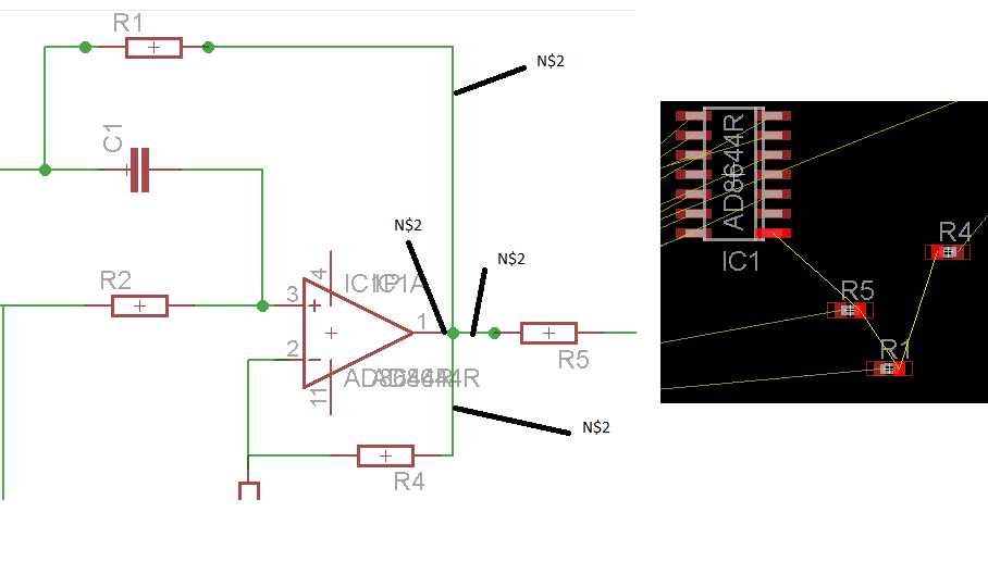
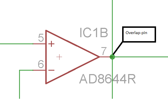
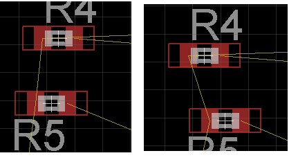
Your assumption is wrong. The net is shown as a daisy chain. The view has in part to do with the specfic operation of the Eagle layout tool, other layout editors will possibly change the "ratnest" or "airline" display according to shortest distance connection when you move the parts around. But you should be able to route the net as you like.

The problem is about learning to manage the tool. Eagle is basically user frienfly and can be (more or less) intuitively operated. A certain learning curve must be granted, however.

It seems like you actually selected small 0402 chip size for resistors and capacitors. Guessing about your skills in electronic craftsmanship, I assume you'll face serious problems to solder this components with acceptable quality. It would be a better idea to recede to a good standard like 0805.
 

Re: first pcb stebs - sallen key filter

Eagle will recalculate the shortest route for the ratsnest if you simply click the 'ratsnest' button. It is useful to do that whenever you move parts around.

Keith
 

Re: first pcb stebs - sallen key filter

I didn't understand very much the answer. Anyway, are you saying that's right that only R5 is connected to the out of opamp ? Recheck the attachment : I underlined the net that I am asking for help. help2.png
 
Last edited:

Re: first pcb stebs - sallen key filter

I didn't understand very much the answer. Anyway, are you saying that's right that only R5 is connected to the out of opamp ? Thx

No, all three resistors need to be connected to the opamp output, but when you have routed all the ratsnest wires then they will be.

Keith
 

Re: first pcb stebs - sallen key filter

so I have to wait to route all the circuit then they will magically appear, right ?
Another point : I can't allineate resistor (see the attachmente). Why ? Thank you all !!!

0_1337183374.png
 

Re: first pcb stebs - sallen key filter

I assume you mean align. If you have moved things around then changed the grid then they will move RELATIVELY based on the new grid. To re-align devices to the new grid, hold down the CTRL key when you click on them for moving. That will snap them to the new grid.

Keith

---------- Post added at 17:13 ---------- Previous post was at 17:10 ----------

Also, you can assign two grids. The alternate grid is selected by holding down the ALT key while you move or route. Normally you would make the alternate grid smaller than the normal grid.
 
Re: first pcb stebs - sallen key filter

Thank you very much ! Another point : How can I connect, in the schematic, two wires with an invisible wire? (look at the attachment to see waht I mean! Of course it was not created by me)


I am not sure what you mean but you can NAME nets. Any net will connect to a net of the same name. So, if you name a net AOUT on one part of the circuit and name another with the same name, even on a different sheet, they will be connected. It is useful to add a net label for any nets named and connected in that way.

Keith
 
Of course it was not created by me
I'm pretty sure you did. E.g. connecting two component terminals and deleted part of the connection later,
 

ok. Now I have a problem in connection. It reports, in the node that you can see in the attachment, "NET$15 overlaps pin" for 4 times (like the number of the wires linked to the out of the opamp). The other op-amps are identical but EAGLE doesn't show any problem for them... THX !!


It is because one of the nets passes over the opamp output pin but isn't connected (the one running vertically I assume). I would suggest you delete all three nets and draw them slightly away from the opamp pin. Personally I avoid crossovers like that anyway, even with junctions but it depends partly on what you think is clear and unambiguous.

Keith
 
It looks pretty bad. Have you run the DRC? There seem to be plenty of short circuits and design rule violations.

Keith.
 

yeah. It was horrible. What do you think about this ?
 

Still look like a lot of shorts and design rule violations.

Has it been auto-routed? I assume not because it shouldn't route with design rule violations.

I think you main problem is component positioning. You need to get that right (by looking at the ratsnest as you move things) before you route it.

Keith.
 

ok. now I resolved the clearance problems. What you think about this ?


really I don't know how to get a less intricate circuit =(
 

Status
Not open for further replies.

Part and Inventory Search

Welcome to EDABoard.com

Sponsor

Back
Top