Continue to Site

Welcome to EDAboard.com

Welcome to our site! EDAboard.com is an international Electronics Discussion Forum focused on EDA software, circuits, schematics, books, theory, papers, asic, pld, 8051, DSP, Network, RF, Analog Design, PCB, Service Manuals... and a whole lot more! To participate you need to register. Registration is free. Click here to register now.

Need code for generating clock doubler using DCM...

Status
Not open for further replies.
dcm rst_in clkin_ibufg_out vhdl

hi,

u said u r facing issues in ur previous projects which worked very much fine earlier.... Did u come to know wheter any issues with ISE or modelsim... Plz let me know if u have any idea about ISE webpack whether it generates good outputs or not?

Added after 1 hours 19 minutes:

Hi,

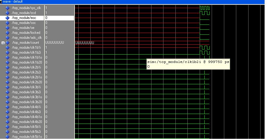
Even though I am getting partial output I mean I am not getting LOCKED output, Still I was simulating design bcz my aim is to get the output clock as twice that of input clock... I am getting error as

# ** Fatal: Integer divide (mod) by zero.
# Time: 1000040 ps Iteration: 19 Process: /top_module/u2/dcm_sp_inst/ps_delay_md_p File: C:/Xilinx/10.1/ISE/vhdl/src/unisims/unisim_VITAL.vhd
# Fatal error at C:/Xilinx/10.1/ISE/vhdl/src/unisims/unisim_VITAL.vhd line 7216
#
run
# Cannot continue because of fatal error.
run
# Cannot continue because of fatal error.
run
# Cannot continue because of fatal error.
run
# Cannot continue because of fatal error.
run
# Cannot continue because of fatal error.
run
# Cannot continue because of fatal error.
run
# Cannot continue because of fatal error.
run
# Cannot continue because of fatal error.

plz check the Output wave form....If u need I wil upload my codes... I have taken my system clock as 100MHZ and input to DCM as 50MHZ....
How do I fix it????????

Added after 1 minutes:


dcm_sp in modelsim 6.4

I suspect the DCM_SP simulation model is broken in ISE 10.1. Xilinx Answer record 30812 says one problem was fixed in SP2, but maybe the fix is incomplete.

I haven't seen any problems with DCM. Try using DCM instead of DCM_SP. However, if you are doing post-route simulations, XST replaces DCM with DCM_SP.

For me, the problem occurs only when using 2X feedback. The CLK2X output is still available when using 1X feedback, but of course the phase alignment will be different. Maybe you can still use it.

I haven't seen the fatal error problem. Try examining line 7216 to see why it's dividing by zero.

Probably the best way to solve your problem is to contact Xilinx support via WebCase. The service is available to registered customers.
http://www.xilinx.com/support/clearexpress/websupport.htm

I've seen related discussions on the Xilinx forums:
http://forums.xilinx.com/xlnx/
 

inst dcm_sp_inst not found. please verify that

Hi,

I have changed DCM_SP with DCM, even then I am getting error. Then I saw the UNISIM file which says PS_delay=1/256 (CLK_IN )period. And with input freq (65 to 125)MHZ should be used acc to datasheets of SPARTAN-3 FPGA.So that PS will lie bit 30 to 60 psec. But as I am doubling clock over six times successively, the outputs at later stages is going beyond range .so I am not getting output till the expected outputs. I am planning to use DFS instead of DCM. But for that PS_delay should lie between 20 to 40 psec. I think I wil end up with same results. will try once....
 

site:edaboard.com vhdl code for clock generator

"even then I am getting error" -- Are you referring to the faulty CLK2X output, or the fatal error messages?

Doubling clock six times? That's 64 times frequency. Long ago you mentioned using a long chain of DCMs. Don't do that! It may work in simulation, but it will probably fail in the FPGA due to accumulated jitter.

What frequency is your input clock, and what output frequency are you trying to generate?
 

dcm 40mhz 50mhz

I am deciding my input clock frequency depending on the DCM (MIN N MAX ) frequency. Bcz I am giving my input to DCM. I am getting clock2x output for only couple of clocks. As my design consists of multiplying clock n num of times. I am instantiating DCM for 6 times and generating ADC clock at the output of 6th DCM.
spartan 3 with DLL got limited freq range. The Output range is beyond the limit
(18 TO 167MHZ for low mode or 48 to 280MHZ). Now I thought I wil use Spartan-3E with DFS which got good freq flexibility between 5 to 333MHZ. even if I give
5 Mhz as my input freq its output at the end of last DCM will be 320Mhz. Plz check my logic block dia and let me know is it going better with DFS?But my DCM with DFS is not working. I tried to generate twice the input freq by selecting (4/2) 4-multiply adn 2-divide so that input is multiplied by 2 as explained in datasheet.If it works I thought i wil directly choose for 6 and 12 multiply numbers, when I instantiate it in top module I got error as ...:cry:


# ** Warning: (vsim-3473) Component instance "clkfx_bufg_inst : bufg" is not bound.
# Time: 0 ps Iteration: 0 Region: /top_module/u0 File: dcm2.vhd
# ** Warning: (vsim-3473) Component instance "clkfx180_bufg_inst : bufg" is not bound.
# Time: 0 ps Iteration: 0 Region: /top_module/u0 File: dcm2.vhd
# ** Warning: (vsim-3473) Component instance "clkin_ibufg_inst : ibufg" is not bound.
# Time: 0 ps Iteration: 0 Region: /top_module/u0 File: dcm2.vhd
# ** Warning: (vsim-3473) Component instance "clk2x_bufg_inst : bufg" is not bound.
# Time: 0 ps Iteration: 0 Region: /top_module/u0 File: dcm2.vhd
# ** Warning: (vsim-3473) Component instance "dcm_sp_inst : dcm_sp" is not bound.
# Time: 0 ps Iteration: 0 Region: /top_module/u0 File: dcm2.vhd
# Loading D:\vidya_projects\dcm-vhdl\libraries\unisim.bufg(bufg_v)
# .main_pane.mdi.interior.cs.vm.paneset.cli_0.wf.clip.cs.pw.wf
# .main_pane.workspace
 

ise 10.1 dcm

Your code is configured for 2X feedback, but you commented-out the CLK2X_BUF lines, so they are probably floating.
Also, we've seen that 2X feedback is probably broken in the DCM_SP simulation model, so try DCM or 1X feedback.

If you use Spartan-3, a 5 MHz input is only allowed in DFS mode.

Why do you want to use such a low input frequency? A DCM causes jitter, cascading DCMs causes even more jitter, and jitter will hurt your ADC acquisition. Also, it may be impossible to use DCMs to convert from 5 MHz to 320 MHz due to excessive jitter. Be sure the output jitter from the first DCM doesn't exceed the allowable input jitter of the next DCM. The ISE Architecture Wizard can tell you the output jitter depending on DCM mode, but it may not calculate accumulated jitter.

VHDL files should have extension .vhd instead of .txt

I don't understand the "is not bound" warnings. Probably some VHDL issue. I use Verilog.
 

instantiating xilinx dcm

okay, as I was using DFS I commented CLK2X output signal in design.
For uploading into EDA I copied my VHDL files in a text file. With clock as input to DCM I am generating ADC-clk so I need very high freq at the output.
 

verilog clock doubler

Your code specified "2X" feedback mode. That mode requires the CLK2X feedback signal. If you don't care about feedback, you can change the feedback mode to "NONE".

I understand your high freq ADC clock. I was wondering why your *input* clock is so low, only 5 MHz. It's more common to use a higher frequency oscillator such as 50 MHz or 100 MHz in FPGA projects, to avoid minimum-frequency limitations and to reduce jitter cause by too much clock multiplication.

You can RAR your vhd files just as easily as txt files.
 

instantiating dcm

Have u worked with DFS? I have decided to used DFS. Bcz with DLL's I need more DCM's its creating unnecessry delay and jitter.
 

xilinx simple example dcm

Yes I've used DFS. Beware that a DFS section generates more jitter than a DLL section. Cascading two DFS sections usually works, but some combinations may not work, so it's not guaranteed by Xilinx. For more explanation, see the comment from the Xilinx fellow in this discussion:
http://forums.xilinx.com/xlnx/board/message?board.id=Virtex&thread.id=911

If you can use 10 MHz input clock instead of 5 MHz, then you would need only one DFS stage to generate 320 MHz.

This example (sorry Verilog) actually works on my Spartan-3E Starter Kit. It divides the on-board oscillator down from 50 MHz to 5 MHz, and then uses two DFS stages to multiply the 5 MHz to 320 MHz. However, the reliability may be marginal because it exceeds the rated specs of my board's "ES" grade FPGA, and I didn't analyze the jitter situation.

Code:
// Pin locations for Xilinx Spartan-3E Starter Kit
module top (clk50MHz, clk320MHz, locked2);
  (* LOC="C9", PERIOD="50 MHz" *) input clk50MHz;
  reg                             [3:0] count = 0;
  wire                                  clk5MHz = count[3];
  wire                                  clka, clkb, clkc, locked1;
  reg                             [4:0] reset=0;
  (* LOC="A10",SLEW="FAST" *) output    clk320MHz;
  (* LOC="A6", SLEW="FAST" *) output    locked2;

  always @ (posedge clk50MHz)
    count <= count == 4 ? -5 : count + 1;   // divide 50 MHz to 5 MHz

  // synthesize 40 MHz from 5 MHz
  DCM dcm1 (.CLKIN(clk5MHz), .RST(1'b0), .CLKFB(), .CLK0(), .CLKDV(), .CLKFX(clka), .LOCKED(locked1));
  defparam dcm1.CLK_FEEDBACK       = "NONE";
  defparam dcm1.CLKFX_MULTIPLY     = 8;
  defparam dcm1.CLKFX_DIVIDE       = 1;
  defparam dcm1.CLKIN_PERIOD       = 200;

  BUFG buf1 (.I(clka), .O(clkb));

  always @ (posedge clkb)
    reset <= {reset,locked1};

  // synthesize 320 MHz from 40 MHz
  DCM dcm2 (.CLKIN(clkb), .RST(~reset[4]), .CLKFB(), .CLK0(), .CLKDV(), .CLKFX(clkc), .LOCKED(locked2));
  defparam dcm2.CLK_FEEDBACK       = "NONE";
  defparam dcm2.CLKFX_MULTIPLY     = 8;
  defparam dcm2.CLKFX_DIVIDE       = 1;
  defparam dcm2.CLKIN_PERIOD       = 25;

  BUFG buf2 (.I(clkc), .O(clk320MHz));
endmodule
 

xilinx dcm verilog

yeah I have downloaded servicepack for 10.1. I will check it out and let u know the results.
 

xilinx dcm unresolved reference

Hi,

I am getting output with DFS in ISE 10.1. Now I am facing the challenge of using two DCM'S. My first DCM has to multiply input clock by six times and second one by two times the output of first DCM. I am not able to generate two DCM'S in one project. I tried with other to use cascade two DCM'S but here its generating dcm module. A popup is opening saying the limited range for DLL and DFS(.200 to 333 MHZ for DFS). But I have only given my clock input as 5MHZ to first DCM, which is multiplied by 6, output is supposed to be 30MHZ then when this is given as input to second DCM which is multiplied by 2 will generate 60MHZ....Even though they are with in the constraints Why it is not taking into consideration...?
 

dfs_frequency_mode unresolved

Which program are you using that generates those error messages? If you are using Project Navigator and Architecture Wizard, sorry I don't build projects that way because of too many headaches. I simply write code like my example above.
 

dcm simulation model

Oh...I mean to say to generate DCM. Are you writing code for DCM by ur own?
 

dcm xlinx cascaded

I write code by hand like my example two messages ago. That's a complete project with two cascaded DFS stages. I don't use any wizards or Project Navigator.
 

dcm_sp component declaration

This you have instatiated from ur DCM module rite generated by ISE..?

DCM dcm1 (.CLKIN(clk5MHz), .RST(1'b0), .CLKFB(), .CLK0(), .CLKDV(), .CLKFX(clka), .LOCKED(locked1));

Here u ahve done port mapping rite?
 

clock multiplication using dcm xilinx

I didn't use any tools to generate that code. I simply read the DCM syntax description in the ISE Libraries Guide, and then wrote the code.

My DCM instantiation statement is quite short because I needed only a few ports. I could make it even shorter by omitting the unused CLKFB, CLK0, and CLKDV ports. I use those ports in other projects, so I kept them here merely as placeholders, reminders to myself. Verilog allows it.

My Verilog example works in simulation and actual hardware. I tested it on my Spartan-3E Starter Kit.
 

dcm locked signal low always modelsim

sorry I didn't get you.... Even though you have written code on your own there should be a lower level module rite? Whats the logic for doubling clock frequency if you are not configuring DCM generated by ISE ?...In your earlier responses you mentioned HDL's won't support?

could you please elaborate it...
 

dcm_sp_inst + vhdl

I simply put all the DCM and BUFG instantiations into my "top" module instead of putting them into separate lower level modules. The code is more compact, one module instead of three. Either way, the design works the same. It can be done in VHDL too, but I'm not very good at writing VHDL.

My code does configure the two DCMs. It uses Verilog "defparam" statements. They are similar to the "generic" statements in your VHDL.

I don't understand "HDL's won't support". If you are referring to my very first message, then perhaps you aren't familiar with the difference between "infer" and "instantiate".
 

clock-doubling counter

you mean to say without DCM being the low level module, u can directly define in top module and just running all the xilinx libraies(unisim,simprim,xilinx corelib) will generate output...? Yeah I don't have much idea about infer, does that mean default consideration?

Added after 6 minutes:

I believe with ur experience over the years in DCM'S have u ever tried to generate two DCM'S in the same project with two different multipliers...? As I am not allowed to generate two DCM'Swith ISE, I wrote the second one using vhdl. Do u have any idea how to define delay elements in VHDL which are synthesizable?
 

Status
Not open for further replies.

Part and Inventory Search

Welcome to EDABoard.com

Sponsor

Back
Top