Continue to Site

Welcome to EDAboard.com

Welcome to our site! EDAboard.com is an international Electronics Discussion Forum focused on EDA software, circuits, schematics, books, theory, papers, asic, pld, 8051, DSP, Network, RF, Analog Design, PCB, Service Manuals... and a whole lot more! To participate you need to register. Registration is free. Click here to register now.

What is maximum possible gain of folded cascode opamp with 180nm CMOS tech .

Status
Not open for further replies.

ASHUTOSH RANE

Member level 2
Joined
Aug 7, 2009
Messages
49
Helped
2
Reputation
4
Reaction score
1
Trophy points
1,288
Location
KOZICODE
Activity points
1,589
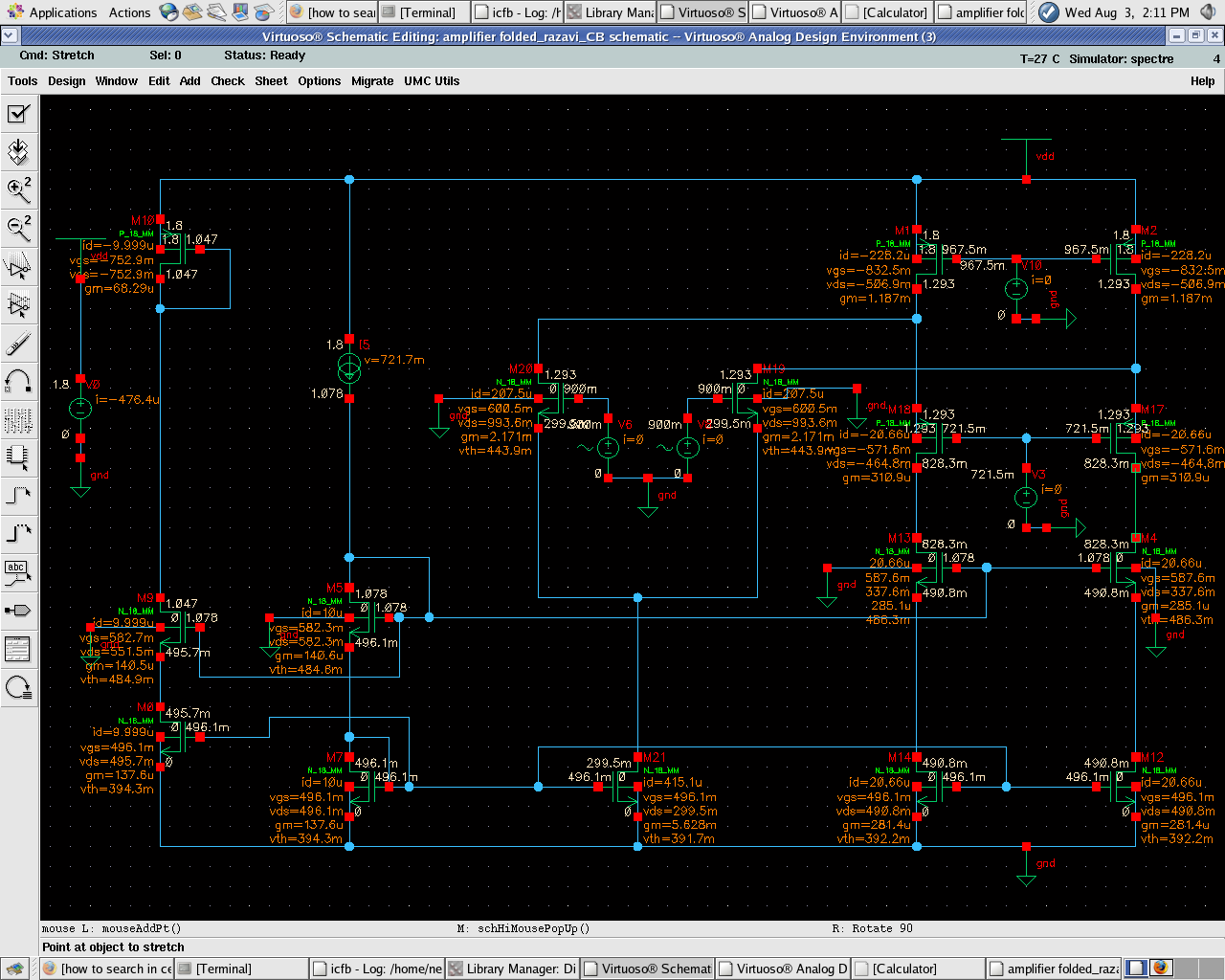
HI friends i am designing the Folded cascode opamp. i am getting maximum gain of opamp as 46 dB..!
@L=900nm and VDD=1.8....if this is the only gain can be obtained then what is good to implement for increasing gain upto 70 dB
1) gain boosting
2)adding one more stage
my GBW requirement is 50MHz and SR is 30v/usec.....what do i do please suggest me


thanks in advance :-?
 

what is L= 900nm? I guess you have access to much smaller lengths in this process or are you using some higher voltage FET?

getting 60-70dB from a folded cascode should not be a problem, which requirements are limiting your design can you explain? what is your gm, Cload, Rout?
 
increase the lengths on the output branch to push up the output resistance. Use the smaller current in the output branch you can with respect to your speed constraints. i think this will increase your gain. If not enough, use gain boosting.
 
u should be able to hit 70dB gain easily using folded cascode design.... 46dB sound likeu dont have transistors biased correctly. use 5-10 times minimum length for current sources/rail devices and 2-3 times minimum L for your cascodes. this will give u good output impedance.
 
hi DGNANI....
Thanx for ur suggestion....i have uploaded the image which defines all details of my design NODE voltages,and operating point of transistor.....
CLoad i have not used...
The Rout is equal to 3.4633 M ohm if i calculate theoretically from simulator obtained gm and gds values of transistors in my design .. also same way i am getting total gain of near by 7K.....
gm is 2.15m i have attached the screen shot for design please let me know where i went wrong ........


Attachments

  • Screenshot-3.png
    Screenshot-3.png
    104.2 KB · Views: 180

Hi Braski
how much smaller current i can use in design to get high output resistance?
 

looking at your schematic, i would recommend you try to have equal currents in the folded cascode branch and in the input transistors. while having low currents generally improves gain it is bad when u have good slew rate requirements.

input diff pair gm can be increased by increasing W/L ratio, this would push the transistors close to sub-threshold and give good gm for lower current.
the current in the nmos current source (M21) will be determined straight from the slew rate , so you will know the minimum current you need in the diff pair, then get the maximum possible gm out of it by increasing W/L. the rest of things will easily fall into place.

a good practice is too design a good bias circuit to bias all the current sources.. it is much better than using DC sources to provide biasing.
 
- consider changing the output stage cascoded NFETs (M4-M13, M12-M14) into a mirror configuration, this will increase gain by a factor of two and also provide other advantages
- the output stage current will be defined by slew rate constraints, which in turn depend on the output capacitance
you can still increase the output resistance by increasing the gm of the cascoded FETs - M18, M17, M1, M2
- for the diff pair you can increase the W/L to push them towards weak inversion
- you have really high gm on the PFET M1 M2, which suggests also high gds; high gm on M1-M2 does not buy much so sacrifice it for a lower gds, lower the gds at least until it matches the gds of the symmetric pair M14-M12

Let us know how it goes...
 
Last edited:
follow dgnani advices! you have to consider your GBW and slew rate constraints!

Hi Braski ,
sorry for not mentioning ...with lowest current i mean current in output branch of folded cascode amplifier.....to get high output Resistance how much low value we can use?
 

- consider changing the output stage cascoded NFETs (M4-M13, M12-M14) into a mirror configuration, this will increase gain by a factor of two and also provide other advantages
- the output stage current will be defined by slew rate constraints, which in turn depend on the output capacitance
you can still increase the output resistance by increasing the gm of the cascoded FETs - M18, M17, M1, M2
- for the diff pair you can increase the W/L to push them towards weak inversion
- you have really high gm on the PFET M1 M2, which suggests also high gds; high gm on M1-M2 does not buy much so sacrifice it for a lower gds, lower the gds at least until it matches the gds of the symmetric pair M14-M12

Let us know how it goes...


hi
Thank u a lot dgnani , for all suggestions ,
-My opamp design target is to design a differential opamp so cannot use current mirror for (M4-M13, M12-M14)....although i have used external current biasing cct for the (M4-M13, M12-M14)....

-i have basic doubt .....my current through the M1 and M2 is high so gm has gone high ...now ....How to reduce gm,and gds of the M1 and M2 ?
 

if the gds of M1-M2 is large compared to M12-M14, M1-M2 will determine the output resistance hence the DC gain: if this is your case, the simplest way to lower gds would be to increase L, you might have to adjust the voltage to make sure everything stays in saturation
 
  • Like
Reactions: ASHUTOSH RANE

    V

    Points: 2
    Helpful Answer Positive Rating

    ASHUTOSH RANE

    Points: 2
    Helpful Answer Positive Rating
hello brothers ,
How much gain we should get at Foldeing node of Opamp that is at drain of M1 and source of M18..... i am getting unity gain at this node ......is it the case for folded cascode design??
 

the gain at the folding node is actually trans-conductance gain ( id = gm(input) * vin )

u have a differential output, u need CMFB ( common mode feedback) to keep output defined else the output node will drift as it is high impedance node. u can use a ideal CMFB and use external load capacitor.
 

Status
Not open for further replies.

Part and Inventory Search

Welcome to EDABoard.com

Sponsor

Back
Top