Continue to Site

Welcome to EDAboard.com

Welcome to our site! EDAboard.com is an international Electronics Discussion Forum focused on EDA software, circuits, schematics, books, theory, papers, asic, pld, 8051, DSP, Network, RF, Analog Design, PCB, Service Manuals... and a whole lot more! To participate you need to register. Registration is free. Click here to register now.

ATMEGA16/32 based single microcontroller inverter with battery charger

Status
Not open for further replies.
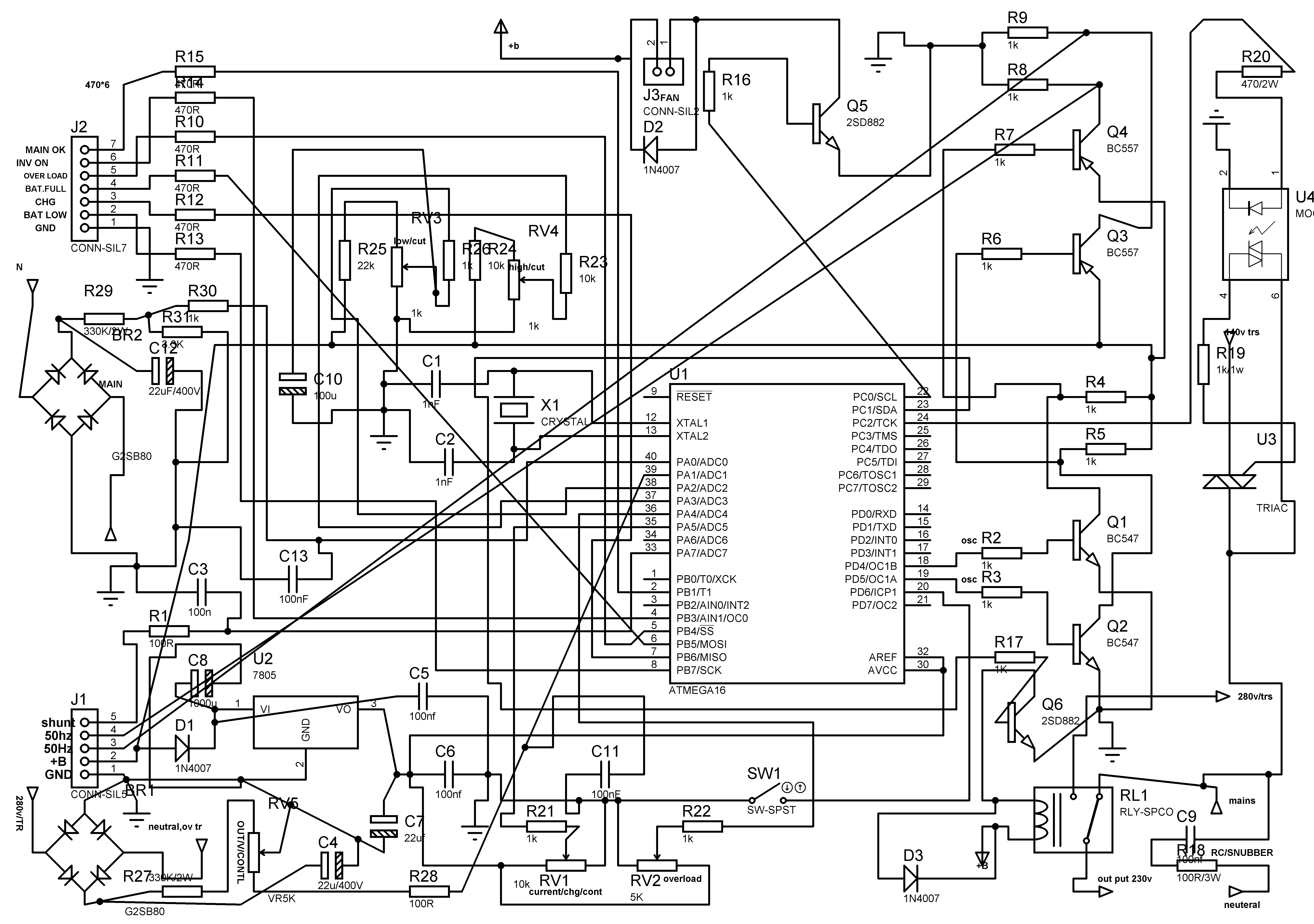
Hi Tahmid as we disscus before,that we can not touch battery terminals in this inverter.I think if we use maintenance free battery(Deep cycle,VRLA etc,) then its ok.
And when we use wet battery with electrolyte,we compell to see water level,specific gravity of acid.
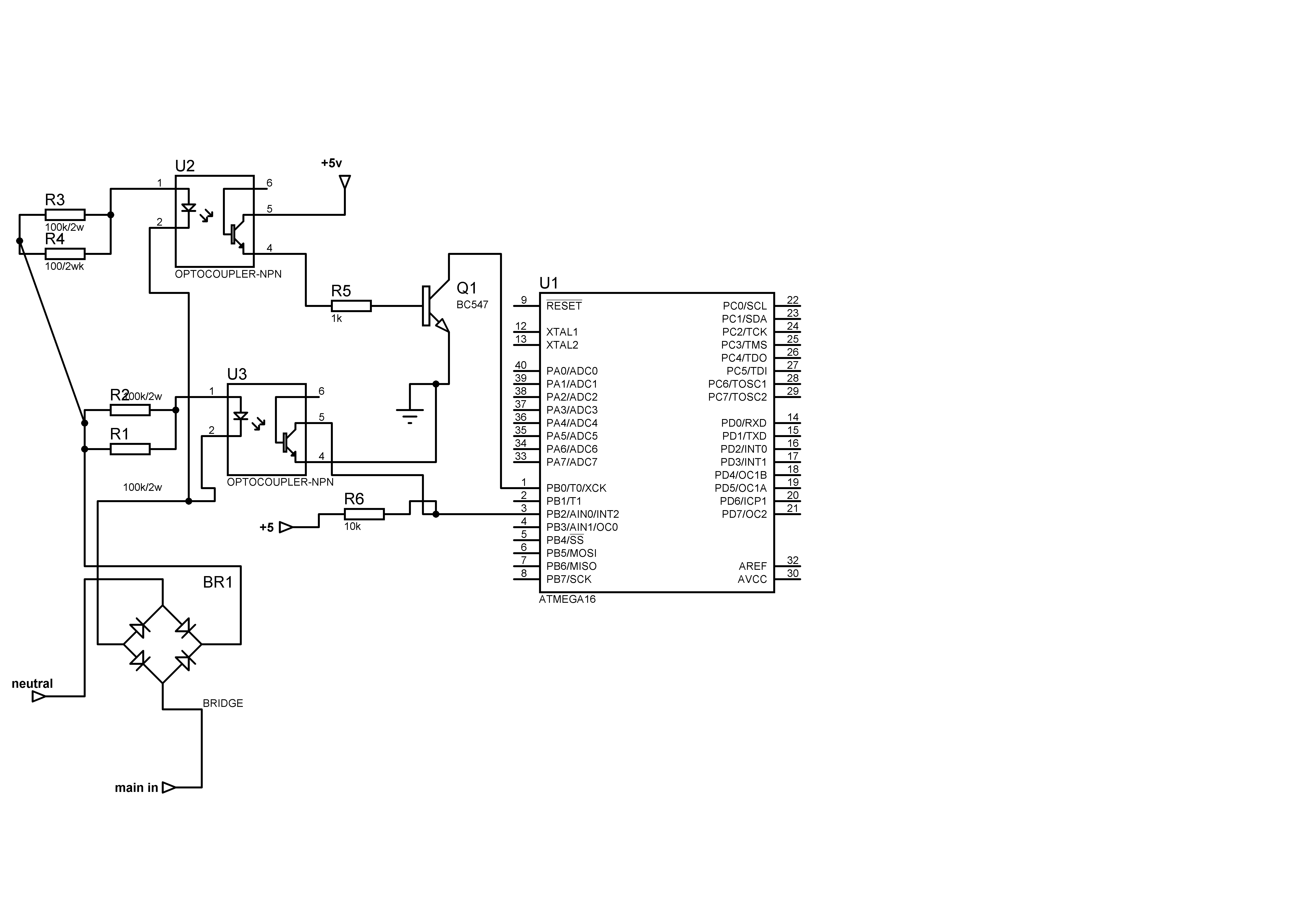
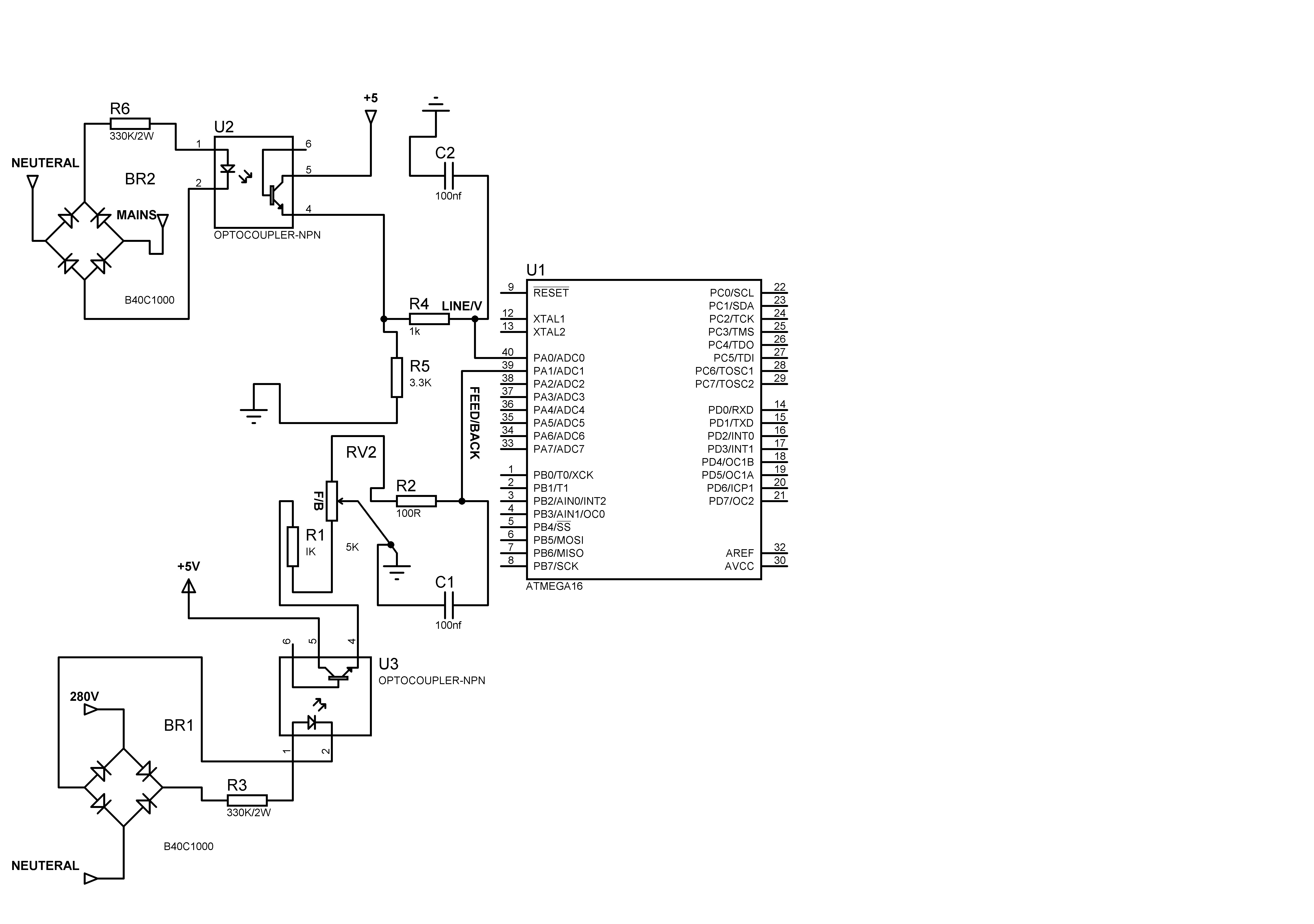
At that time we need isolation between negtive of battery,and negtive of mains(through bridge,1n4007).
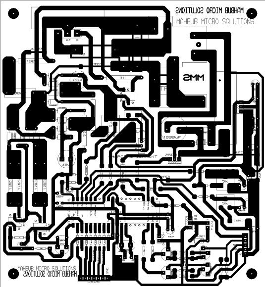
I have try to modify a few in your inverter,s schematic.
I hope after modification,we can touch battery terminals,and maintain battery without fear of electric shock.
As you said that we need almost 2.5v dc at pin number 39,40(ADC-INPUT).
Yes we can get isolated dc volts(0 to 4) from pin number 4 of optocouplers.
with best wishes
Hi,
The voltage can be adjusted as required. Currently, it's set to 2.5v. Can you please explain your suggestion?

Thanks.
Tahmid.
 

Hi Tahmid,
I think we can address the issue of overload/short circuit protection, can you suggest a reliable/effective
protection for a mosfet-based inverter. i need practical circuit with short explanation of how it works.
What is the difference between overload and short-circuit?. is desaturation network possible with mosfet
design if yes pls. show a simple one for bridge inverter

regards
 

Hi pnjtbr,
Your circuit provides isolation and allows for varying voltage but the feedback is not load compensated and line voltage can not be measured with what you've shown here.

Tahmid.
 

Hi Tahmid,Actually i derived idea from your schematic.
As you already using 2 opto-couplers in your schematic,one for MAINS sense and 2nd,
for zero crossing detection.
You mean if we modify the schematic like this,we only can get isolation.
And we can not fix output volts(in inverter mode).
Can you send me hex file?
I have to try this circuit.
I also note that we can extand some features in it.
As we have pin 25 to pin 29(PC3 to pc7) empty.
We can show here battery level indicator with 5 leds.
Best regards.
Hi pnjtbr,
Your circuit provides isolation and allows for varying voltage but the feedback is not load compensated and line voltage can not be measured with what you've shown here.

Tahmid.
 

Attachments

  • main sense and zero cross detection.bmp
    3.1 MB · Views: 292
Last edited:

Hi Tahmid
Can you please upload your schematics so that we can all make well informed remark and contribution on it.
We can equally learn one or two things there.I hope also you will respond to my overload/short circuit request

Regards,
 

    V

    Points: 2
    Helpful Answer Positive Rating
Hi Tahmid,
Can we have your reply?

Regards
 

I think tahmid is very busy now, just give him some time he will post it.
 

He will not post the schematics if he does he will not give the hex file of the atmega16/32 so is useless demanding for the schematics.
 

He will not post the schematics if he does he will not give the hex file of the atmega16/32 so is useless demanding for the schematics.
May be with the schematic and with a good understanding of how the circuit works the user could write there own code for it or even use the basics for the deisgn and use a Picmicro instead to control it(this the way I would go has I've never used AVR). Life is full of chalanges. :)
 

Hi,
Yes, I agree with wizpic. I am out of town for the last few days. I will post schematics when I get home.
 
  • Like
Reactions: wizpic

    wizpic

    Points: 2
    Helpful Answer Positive Rating
@ wizpic,
Hi,
I have a plan to design one using PIC as well, but this has to wait as I just don't have the time now.
Anyway, those who are proficient in PIC programming can easily design one themselves using the ideas used and discussed here. Plus, the schematic, PCB and design offer room for much improvement which can be used in other designs as well. I hope to improve on this design using both PIC and AVR when I get time and this would be beneficial to many.

Tahmid.
Is this for the inverter or charger or both, I can layout the PCB for it if needed
 

Design of your pcb is ok.I think design of pcb depend upon size of cabinet of inverter.
First we should see which side of inverter,s box have leds,output socket,fuse holders,hole for battery bus bar and mains supply cord.Than we can start better pcb layout design.
Header for leds,and for power mosfet board are at right place in your design.
only conection of power transformer loops are looking different,these should be at outer edge of pcb.
Hi,
It's for both. It would be great if you could help with PCB.
 
Last edited:

Hi,
It's for both. It would be great if you could help with PCB.

Sure No problem I see what I can do, I shall look at all the options and think of other members who may want to build it


wizpic
 

We could work together and develop a PIC based inverter.
Anyway, about the schematic, I need some time to draw it, I'll do that and upload it within a few days.
 

That's sound nice tahmid,then let's start working on it.
 

Yes, let's get started. Where should we start from?
As for the schematic, I hope someone can help me trace that from the PCB, or else you'll have to wait, as I'll need to draw it and I don't get much time free these days.

Tahmid.


I draw in a very small period,some lines may not clear,but this schematic is according to pcb lay out.
Yes, let's get started. Where should we start from?
As for the schematic, I hope someone can help me trace that from the PCB, or else you'll have to wait, as I'll need to draw it and I don't get much time free these days.

Tahmid.
 

Attachments

  • tahmid,s inv_bitmap.jpg
    1.9 MB · Views: 171
  • main sense and zero cross detection.jpg
    597.3 KB · Views: 132
Last edited:
Hi,
Thanks a lot for that. But for some reason, I can't view the picture. It stops loading half way through. Thanks for taking the effort.
 

Status
Not open for further replies.

Similar threads

Part and Inventory Search

Welcome to EDABoard.com

Sponsor

Back
Top