Continue to Site

Welcome to EDAboard.com

Welcome to our site! EDAboard.com is an international Electronics Discussion Forum focused on EDA software, circuits, schematics, books, theory, papers, asic, pld, 8051, DSP, Network, RF, Analog Design, PCB, Service Manuals... and a whole lot more! To participate you need to register. Registration is free. Click here to register now.

[Moved]: Ultra-low Power Bandgap Reference design

Status
Not open for further replies.
The regulator that I have included below shows a relatively simple topology that will step down the input voltage to the reference voltage of the bandgap plus an additional factor of the resistor ratios.


The output voltage is:

Vout=(1+R2/R1)Vref

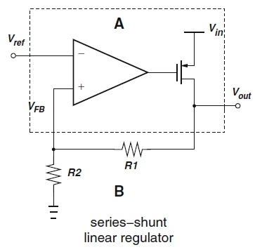
No, it will step up the input voltage of course, and the output voltage is Vout=(1+R1/R2)Vref
 
  • Like
Reactions: zilch

    zilch

    Points: 2
    Helpful Answer Positive Rating
Oh! I'm sorry, that's what I meant to say. Thanks for correcting me :)
 

Hi ljp, sorry for the confusion. Before I posted this thread, our initial plan was to boost the output from the rectifier which we assumed that it's only around 0.3V output (or lower) by using a charge pump to step up the overall output voltage to serve as a supply for sensors. That's why I am designing a BGR with low supply. But we found an architecture that the output of the rectifier can be improved up to 1V or higher, so I decided to increase the voltage of BGR and use LDO to provide a stable output. Basically, this is what we are trying to do. block-diagram.png
 

Sorry, that block diagram is wrong. Both control ckt and battery should be at the end. So we are basically charging the battery so it can serve as a supply for sensors. I hope i made it clear.
 

Okay, that makes more sense to me then. I think if you use that LDO you shouldn't have too many problems. If you've got any other questions, I'll gladly help!

Good Luck!
 

In this case, should we focus on the current produced by the LDO to charge the battery?
 

There are other topologies that can provide a constant current source depending on a resistor ratio which you could always use to charge the battery.
 
  • Like
Reactions: zilch

    zilch

    Points: 2
    Helpful Answer Positive Rating
Hi ljp, do you have any suggestions or could you point me in the direction of some useful resources of LDOs with current limitation? Actually I have found one, "A Sub-1V CMOS LDO Regulator with Multiple Protections Capabilities" by Hung and Ceng. I dont know if this will be a good source to follow.
 

That paper looks good, I was going to suggest that topology actually, I wasn't sure how much protection your circuit would need, but the image I have attached shows the bare minimum, the input signal can be your DC Bias point from the bandgap and you can choose a resistor value to set the current.

In an ideal op-amp, the voltage differential across the two terminals is zero and vref is essentially "placed" on the other terminal which forces the voltage across the resistor. In accordance with Ohm's Law, your current is now:

Iref=Vref/R


EDIT:


Sorry, one other thing about this circuit(which I pulled from the web)...

I would use a PMOS device with source tied to VDD and you would need to connect Vref to the negative terminal of the op-amp and the positive terminal is connected to the drain of the PMOS device. It looks like positive feedback but it is not, in reality you have a common source attached to the op-amp which gives you an additional phase inversion.

The reason I would choose this topology is that it is easier to remain in saturation as you only require a VDS drop.
 

The paper I suggested is a bit of a challenge. The W/L ratio is 1:1000. I don't know if it's possible in the technology that I'm using.
 

The W/L ratio is 1:1000. I don't know if it's possible in the technology that I'm using.

1000:1 , probably. Possible in any technology. 100 fingers at W=10 , e.g.
 

Considering the simplest topology of LDO, can I get a reasonable efficiency?
 

I had overlooked that part. That seems insane for any technology for a single device at least. But one thing you can do is this:

Make MP1 a non-unity value such as 50. Then MP2 would only need to be 1/20.

In any case, the reason as to why the aspect ratio is so large is to reduce power consumption. You can probably play around with the ratios to find an optimal tradeoff between area and power. Your power supply of 0.45V is half of what the paper used, so you might be able to get acceptable results. If not, I would still use this LDO but with a different current limiter structure.

You don't really want to mess around with self-cascoding, source-degeneration, or diode drops in this case since the current limiter circuit is a translinear loop of sorts.

Simulate the circuit and determine if the efficiency is acceptable, if not you just need to refine the design.
 
  • Like
Reactions: zilch

    zilch

    Points: 2
    Helpful Answer Positive Rating
Sorry, I did not read it clearly. It says on the paper (W/L) of Mp2 = (1/1000)(W/L) of Mp1

- - - Updated - - -

Your power supply of 0.45V is half of what the paper used, so you might be able to get acceptable results. If not, I would still use this LDO but with a different current limiter structure.

Update: The output of our rectifier is around 1.4V. And the battery that we are going to use is NiMH, which requires to be charged in a constant current.

- - - Updated - - -

What's the difference of Digital error amplifier to other error amps?
 

I am actually not familiar with digital error amplifiers, do you have a reference I can look at?

But as this is an analog circuit, you would want to use a traditional error amplifier. Are you looking at error amplifiers for the opamp in the LDO? A typical high gain amplifier will do the trick. Depending on the intrinsic gain in your process(not sure what you're working with) you might need to resort to cascoding. A good starting point would be a simple differential first stage with a common source second stage. If that doesn't do the trick go for a folded cascode first stage with a Monticelli class AB biased output stage(which also happens to be the industry standard for a high gain rail-to-rail amplifier).
 

Screenshot_20.png


I'll be using this topology. I think this is enough.
 

Looks good to me, you might have voltage headroom issues on the constant transconductance bias portion of the circuit if you're using 0.45V. 1.4v should be fine if you use that.

Also, if your process is a single well p type substrate process you won't be able to tie the body to the source as in the schematic there if it's an NMOS device for that output compensation capacitor.
 

I've set the voltage to 1V minimum. Also, I am using LVT MOSFETs and I'm not sure if I'm doing this right.
 

What exactly are you not sure if you're doing right?
 

I've read that when using LVTs, the leakage current will be large.

On the amplifier side, I've reach a gain of around 60dB. I don't know if this is enough, it's difficult to attain a gain of atleast 75dB.
 

Status
Not open for further replies.

Part and Inventory Search

Welcome to EDABoard.com

Sponsor

Back
Top