Continue to Site

Welcome to EDAboard.com

Welcome to our site! EDAboard.com is an international Electronics Discussion Forum focused on EDA software, circuits, schematics, books, theory, papers, asic, pld, 8051, DSP, Network, RF, Analog Design, PCB, Service Manuals... and a whole lot more! To participate you need to register. Registration is free. Click here to register now.

[SOLVED] Altium doesn't save some changes related to soldermask. Bug?

Status
Not open for further replies.

Lucast85

Member level 3
Joined
Oct 19, 2009
Messages
62
Helped
4
Reputation
8
Reaction score
4
Trophy points
1,288
Location
Italy
Activity points
1,966
Hello,

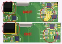
I've a problem with Altium designer during PCB design.
I've finished to design a 4-layer board and I find 2 mistakes. See the below image:

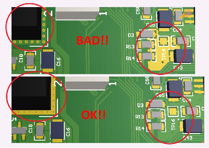
  1. In the top-left red circle there's a lack of soldermask. The black block is an heatsink and the footprint of the heatsink is composed by many vias and two copper regions (one in solder layer, the other in component layer). I set-up a soldermask expansion in the component side of the footprint to fix this problem and leave a region without soldermask under the heatsink. All goes well (see the second image, marked as "OK!!").
  2. In the bottom-right red circle there's a lack of soldermask in the copper polygon pour on the component side. But...why? I fix it rebuilding the polygon. As second image shown all goes well.
Finally I saved all the project's files.
When I open the project again, it seems the changes were not saved. Why?
P.S. Other changes instead were correctly saved!

Anyone can help me? Maybe a bug or I did something wrong?
Thank you all!
 

Are there any primitives on the top solder mask layer? When exactly does the solder mask cutout appear?
If you export gerbers, are these correct (i.e. perhaps it is a 3D rendering bug)?
 

Are there any primitives on the top solder mask layer?
NO.
When exactly does the solder mask cutout appear?
Every time I open Altium designer by clicking into Altium's icon on my desktop (last workspace is opened) after a saving of all files (with a correct soldermask) was done.
If you export gerbers, are these correct (i.e. perhaps it is a 3D rendering bug)?
Yes, they're correct. They reflect the actual (bad) status of soldermask I see in 2d and 3d view of PCB: it isn't a rendering bug.
If I generate the Gerber once I've corrected the two problems, the Gerber are OK. But if save all, close Altium and re-open the project, the soldermask has the cutout zone thus I must fix the problems everytime I open Altium. It bother me!!
 
Last edited:

Very strange, no idea what the problem is. This definitely shouldn't be happening, so I suspect a bug.
 
Using new Altium 15 the strange behavior disappear! Probably was a bug...
 
Thanks for the feedback, and glad your issue is solved!
 

Status
Not open for further replies.

Part and Inventory Search

Welcome to EDABoard.com

Sponsor

Back
Top