Lucast85
Member level 3

- Joined
- Oct 19, 2009
- Messages
- 62
- Helped
- 4
- Reputation
- 8
- Reaction score
- 4
- Trophy points
- 1,288
- Location
- Italy
- Activity points
- 1,966
Hello,
I've a problem with Altium designer during PCB design.
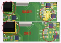
I've finished to design a 4-layer board and I find 2 mistakes. See the below image:

When I open the project again, it seems the changes were not saved. Why?
P.S. Other changes instead were correctly saved!
Anyone can help me? Maybe a bug or I did something wrong?
Thank you all!
I've a problem with Altium designer during PCB design.
I've finished to design a 4-layer board and I find 2 mistakes. See the below image:

- In the top-left red circle there's a lack of soldermask. The black block is an heatsink and the footprint of the heatsink is composed by many vias and two copper regions (one in solder layer, the other in component layer). I set-up a soldermask expansion in the component side of the footprint to fix this problem and leave a region without soldermask under the heatsink. All goes well (see the second image, marked as "OK!!").
- In the bottom-right red circle there's a lack of soldermask in the copper polygon pour on the component side. But...why? I fix it rebuilding the polygon. As second image shown all goes well.
When I open the project again, it seems the changes were not saved. Why?
P.S. Other changes instead were correctly saved!
Anyone can help me? Maybe a bug or I did something wrong?
Thank you all!
