Continue to Site

Welcome to EDAboard.com

Welcome to our site! EDAboard.com is an international Electronics Discussion Forum focused on EDA software, circuits, schematics, books, theory, papers, asic, pld, 8051, DSP, Network, RF, Analog Design, PCB, Service Manuals... and a whole lot more! To participate you need to register. Registration is free. Click here to register now.

Which one is the correct one?

Status
Not open for further replies.

AMSA84

Advanced Member level 2
Joined
Aug 24, 2010
Messages
577
Helped
8
Reputation
16
Reaction score
8
Trophy points
1,298
Location
Iberian Peninsula
Activity points
6,178
Hi guys,

As I say in the topic, which of these two is the real NOR gate? Basic question but I have seen two different cofigurations:

1111111.png

Regards.
 

I don't see a difference except for flipped position of two MOSFETs which is meaningless.
 

Both are 'real' NOR gates, the difference comes when there are two types of inputs.

For example, lets say that you have two inputs,
1. A fast switching signal(like a clock),
2. A slow switching signal(like some control).

Both these go to the PMOS which are in series.

Having the clock input at the top PMOS would increase the delay to the output.
So it is better to have the control signal on top since it would be switching less.
 
  • Like
Reactions: AMSA84

    AMSA84

    Points: 2
    Helpful Answer Positive Rating
Having the clock input at the top PMOS would increase the delay to the output.
So it is better to have the control signal on top since it would be switching less.
How much difference in propagation delay and rise tiime do you expect? I wonder if it's significant in relation to process variations?
 

It is just a 'good practice', I have not actually calculated out the difference...
And apparently it adds less jitter/noise on the clock than when it is connected the other way around.

But we do it for things like Muxes, Gates etc which use a control signal to control a Fast Clock.

That is the only difference between the two that I can see.
 
  • Like
Reactions: AMSA84

    AMSA84

    Points: 2
    Helpful Answer Positive Rating
Having the clock input at the top PMOS would increase the delay to the output.
So it is better to have the control signal on top since it would be switching less.

How much difference in propagation delay and rise tiime do you expect? I wonder if it's significant in relation to process variations?

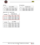
Here are prop. delays from the Oct-2001 Artisan Std.Lib. for several NOR2 gates: Artisan-Lib_NOR2.png

XL .. X4 are NOR2 gates with different fanout.

A is the input to the upper PMOS. As you can see, the A input's intrinsic delay - for the same output change - is slightly shorter than the B input's, whereas their load-dependent delays are practically the same.
 
Status
Not open for further replies.

Part and Inventory Search

Welcome to EDABoard.com

Sponsor

Back
Top