Continue to Site

Welcome to EDAboard.com

Welcome to our site! EDAboard.com is an international Electronics Discussion Forum focused on EDA software, circuits, schematics, books, theory, papers, asic, pld, 8051, DSP, Network, RF, Analog Design, PCB, Service Manuals... and a whole lot more! To participate you need to register. Registration is free. Click here to register now.

[SOLVED] DRC issue in AMS 0.35 µm HV

Status
Not open for further replies.

K4R1

Newbie level 6
Joined
Jan 8, 2014
Messages
12
Helped
2
Reputation
4
Reaction score
2
Trophy points
3
Activity points
80
Hello all,

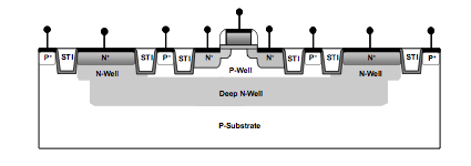
I have 2 DRC errors that i do not understand in my layout. I am actually routing a very simple inverter but using a HV NMOS, with a protective diode on the bulk. And since the layout of this transistor do not looks like the one we have usually when we use a common HV MOS, i am a bit confused.

Here are the 2 messages i do not understand:

"DNR002: Utmost structures within DNTUB must be closed NTAP rings in SNTUB"

"SNR005: RPTUB shape in DNTUB is totally outside sntub ring Each RPTUB shape inside DNTUB must be fully enclosed with SNTUB"

Many thanks for your help and time.
 

"DNR002: Utmost structures within DNTUB must be closed NTAP rings in SNTUB"
All structures within DNTUB (deep n-well) must be enclosed by NTAP (n+) rings in SNTUB (shallow n-well)


"SNR005: RPTUB shape in DNTUB is totally outside sntub ring Each RPTUB shape inside DNTUB must be fully enclosed with SNTUB"

RPTUB (p-well) shape found in DNTUB (deep n-well) which is totally outside sntub (shallow n-well) ring. Each RPTUB shape inside DNTUB must be fully enclosed with SNTUB.

See this cross-section:
 
  • Like
Reactions: K4R1

    K4R1

    Points: 2
    Helpful Answer Positive Rating
Many thanks for the reply.

Actually, does it mean that i have to draw a PD_N via around the transistor and draw a SNTUB around it ? What are the layers used to draw the NTAP ?

Thanks for your time.
 

... does it mean that i have to draw a PD_N via around the transistor and draw a SNTUB around it ? What are the layers used to draw the NTAP ?

I don't know the layer names of the AMS 0.35 µm HV process, sorry. Yes, it means that you have to draw an n-well (SNTUB) ring around it, with an n+ tap contact ring within it, contacting it by vias to metal_1 and your highest VDD. See my explanation and the figure above.
 
Ok, i got it ! Actually, here is how i solved the problem: Draw a "ndiff_rptub" guard ring around the transistor with the automated ring creator in Layout XL. Solved my issue !

Many thanks for the help !
 

By the way, i was wondering ,what is the physical explanation for having a RPTUB ring outside a DNTUB ? Why is an HV MOS not like a regular MOS in 0.35 µm ??!
 

... what is the physical explanation for having a RPTUB ring outside a DNTUB ? Why is an HV MOS not like a regular MOS ... ??!

This is a guard ring, well appropriate to catch and feed straying holes to GND. This is to prevent thyristor action between the HV nMOS and a (possibly) nearby pMOS in the substrate.

HV MOS transistors operate with higher electric fields than regular (LV) transistors, thus creating larger space-charge regions and leakages, by this more straying charge carriers which could trigger thyristor action, i.e. latch-up.
 

Re Hello,

I have an other question related to the layout of an isolated MOS. Actually, i am trying to route the two transistor circled in red and connect the diode linked on the bulk. But i do not understand which part of the blk connection i am supposed to connect to my high voltage so the diode can be biased ? I am trying to connect the green squared bulk connection to the metal 2 but it does not seems to be working...

Many thanks for your help.

see below in the picture to understand what i mean:

lay.jpg

- - - Updated - - -

Ohhhh... actually i solved it, my problem was that i putted two transistors with two different bias voltage on each bulk... Remember this rule of thumb for those in my case: one rptub ring = one voltage on the bulk inside !!
 
  • Like
Reactions: erikl

    erikl

    Points: 2
    Helpful Answer Positive Rating
Status
Not open for further replies.

Part and Inventory Search

Welcome to EDABoard.com

Sponsor

Back
Top