Continue to Site

Welcome to EDAboard.com

Welcome to our site! EDAboard.com is an international Electronics Discussion Forum focused on EDA software, circuits, schematics, books, theory, papers, asic, pld, 8051, DSP, Network, RF, Analog Design, PCB, Service Manuals... and a whole lot more! To participate you need to register. Registration is free. Click here to register now.

simple Cascode amplifier design

Status
Not open for further replies.

ghasem_008

Full Member level 4
Joined
Feb 9, 2012
Messages
221
Helped
11
Reputation
22
Reaction score
10
Trophy points
1,298
Activity points
2,990
Hi.
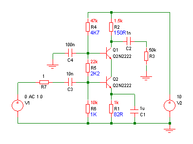
I have to design a simple cascode BJT amplifier.
The last time that I've read electronic circuits is about three years ago and now forget it.
is there anyone who design it for me and simulate with ADS or Pspice software?
thank you very much...
cascode.png
 

how use from given bandwidth to specify capacitors?
 

I don't think you can meet all the requirements. There's a tradeoff between bandwidth, gain and power consumption. The results of some simulations are shown below.

With the resistor values shown in red, the power consumption is about 7.7mW, but the bandwidth is only about 40MHz, as shown by the red trace.

Reducing the resistors to the values shown in blue increases the bandwidth to about 200MHz (as shown in the blue trace), but the power consumption rises to about 84mW.

If you juggled the values just right, you could probably get about 60MHz bandwidth with 10mW power consumption.

The problem is that the upper -3dB point is set by the output capacitance of the top transistor, and it's collecter resistor (Rc in your diagram, R2 in mine).

Reducing the value of that resistor pushes the -3dB point to a higher frequency, but also reduces the overall gain. The only way to increase the gain back to the desired value is to run the bottom transistor at higher current, which increases the power consumption.

To simultaneously meet the requirements of 30dB gain, 120MHz bandwidth and 10mW power consumption, you'd need to look for a transistor with significantly lower output capacitance.

btw, Is this just a homework assignment, or do you actually want to make an amplifier? I ask because the source and load impedances given are extremely unusual, if not completely impractical for an RF circuit. Also, "β=150" is the sort of idiot thing I've only ever seen in classroom exercises.

 
"β=150" is the sort of idiot thing I've only ever seen in classroom exercises.
The teacher bought thousands of 2N2222 transistors and tested the hFE of each one to find two with an hFE of 150.
OOPs, none did so the teacher bought thousands more and tested them too.
 

I don't think you can meet all the requirements. There's a tradeoff between bandwidth, gain and power consumption. The results of some simulations are shown below.

thank you for your attention.I know that there is a tradeoff between gain & BW.can you tell me how you use from BW in this design?Bypass and Blocking capacitors are related to "lower 3 dB frequency".while BW is approximately equal to "upper 3dB frequency".
Also,can you attach your simulation details?

- - - Updated - - -

btw, Is this just a homework assignment, or do you actually want to make an amplifier? I ask because the source and load impedances given are extremely unusual, if not completely impractical for an RF circuit. Also, "β=150" is the sort of idiot thing I've only ever seen in classroom exercises.
Yes,It is only a homework assignment.as you said,source and load impedances are unusual.
 

Also,can you attach your simulation details?
I aready did.

What other details do you want?

- - - Updated - - -

Yes,It is only a homework assignment...
Why don't you do the simulation yourself? Surely you have simulation software if your studies require you to do simulation?
 
Last edited:

OK. Before that let's do a calculation of the transistor's transconductance, since we'll need that for a couple of other calculations.

Since the collecter current is about 0.65mA, the transconductance is given by:
gm = 0.65mA/26mV = 25mMho
i.e. a 1mV change in vBE will result in about a 0.025mA change in collecter current.
For the calculations below, it's more convenient to think in terms of the dynamic emitter impedance Re = 1/gm = 40 Ohms

----------------------------

Capacitors:

There are three low frequency rolloffs. Referring to my schematic, and the red resistor values:

a) A rolloff caused by C2 and the series combination of R2 and R3. That gives a rolloff with -3dB at F = 1/(2*pi*51.5K*1nF) = 3.1KHz

b) A rolloff caused by C1 and the parallel combination of R1 and Re of the bottom transistor. That gives a rolloff with -3dB at F = 1/(2*pi*38.5Ohms*1uF) = 4.1KHz

c) A rolloff caused by C3 and the parallel combination of R5, R6, and the input impedance of the bottom transistor, which is approximately hFE*Re = 150*40Ohms = 6k. That gives a rolloff with -3dB at F = 1/(2*pi*3.2K*10nF) = 5KHz

Since (b) and (c) are fairly close, there will be some interaction. To accurately calculate the rollof at the input, one should take into account the effect of C1 on the input impedance of the transistor. Unfortunately, I don't have a handy formula for that.

The value of C4 isn't critical. I arbitrarily made it 10 times C3 to minimise the signal voltage at the base of the top transistor at low frequencies.

I didn't bother, but it's probably a good idea to set the rolloffs due to C1 and C2 at lower frequencies than that due to C3. That way the dominant rolloff is right at the input.

-------------------

Gain:

The voltage gain of the circuit is approximately given by the load impedance (i.e. the parallel combination of R2 and R3) divided by Re of the bottom transistor.
Gain = 36.4 => 31.2dB

Design steps:
1) Decide what the quiescent current of the transistors should be
2) Calculate Re
3) Calculate R2 = Re * desired voltage gain

------------------------------

Bias resistors:

There's a few considerations when choosing R4, R5 and R6:

a) Higher current through the transistors will result in better gain-bandwidth. Since the total current consumption is limited, don't use too much for the bias network. More current through the bias resistors means less through the transistors.

b) It's a good idea to design for at least a few hundred mV across R1, so the current through the transistors won't change much if the vBE of the bottom transistor is different to what you expected by 50mV or so.

c) In general, any transistor needs at least a couple of volts between collecter and emitter to perform well.

d) In this circuit, the bandwidth is limited by the collecter-base capacitance of the top transistor. Since the capacitance reduces with increasing voltage, it makes sense to have as much voltage across that transistor as possible.
 
dear godfreyl!
thank you...
I have two question:
1. in theory,how do I have to calculate upper 3dB frequency,while high frequency capacitors are related to 2N2222A?in fact,how did you understand theoretically that upper frequency is larger than 40 MHz in this circuit?
2. what is your suggestion for the top transistor?which transistor is best for this purpose?

- - - Updated - - -

what is mean of "Dc power dissipation"?
do I have to account loss in transistors?namely:
Dc power dissipation = Power (resistors) + loss power(transistors) in DC analysis?
 

1. in theory,how do I have to calculate upper 3dB frequency,while high frequency capacitors are related to 2N2222A?in fact,how did you understand theoretically that upper frequency is larger than 40 MHz in this circuit?
Good question, embarassing answer.
Basically, I believed the simulation result and didn't bother to check. Now that I looked in the datasheet, I see that the output capacitance is typically about 5pF with vCE = 5V (see graph below). With a collecter resistor of 1.5K, that would give an upper -3dB point of about 20MHz. What's worse is the datasheet also says that the maximum output capacitance at vCE = 10V is 8pf, about double the "typical" value. So if you happen to get a specimen with higher than the "typical" capacitance, the bandwidth will be less than 20MHz.

There's an important lesson there: Don't blindly trust simulation results - some of the transistor SPICE models used are very inaccurate.

Oh, wait - here's another lesson: If you take a closer look at the graph below, you'll notice that the x-axis is labelled wrong - Onsemi screwed up on the datasheet. So don't believe everything you see in datasheets either, they sometimes have printing mistakes. When in doubt, check a couple of datasheets to see if they agree. (I did, they do, that really is the output capacitance)

2. what is your suggestion for the top transistor?which transistor is best for this purpose?
That's a difficult question. All the old through-hole high-frequency transistors seem to be obsolete/no longer available. I couldn't find any in the RS online catalog at any rate. They do have a lot of SMD parts which may be suitable, but I,m not familiar with any of them.

[grumble]
Coming back to to electronics as a hobby after about 20 years, it's sad to see the whole industry moving towards surface-mount parts which I can barely see, let alone solder. And that new-fangled lead-free solder that doesn't work properly, and doesn't look right even when it does work.
[/grumble]

- - - Updated - - -

what is mean of "Dc power dissipation"?
The picture in post 1 says "DC power dissipation: PD < 10mW", so the total power drawn from the power supply must be less than 10mW. Since the supply is 10V, that means the circuit should not draw more than 1mA of current from the supply.
 
Don't blindly trust simulation results - some of the transistor SPICE models used are very inaccurate.

Onsemi screwed up on the datasheet. So don't believe everything you see in datasheets either, they sometimes have printing mistakes.

Coming back to to electronics as a hobby after about 20 years, it's sad to see the whole industry moving towards surface-mount parts which I can barely see, let alone solder. And that new-fangled lead-free solder that doesn't work properly, and doesn't look right even when it does work.
I agree (and here are some extra characters so the total is more than 10).
 

Status
Not open for further replies.

Similar threads

Part and Inventory Search

Welcome to EDABoard.com

Sponsor

Back
Top