Continue to Site
Follow along with the video below to see how to install our site as a web app on your home screen.
Note: This feature may not be available in some browsers.
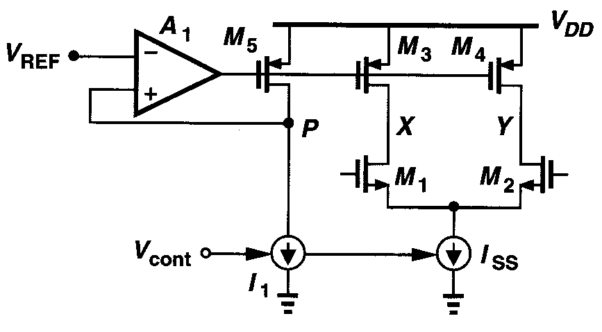
The circuit is called "Regulated drain current Mirror". It increases the output impedance and any variation makes output voltage constant.
Yes. ZekeR gave a good answer in post 2.Anyone has another answer?
Need not to be , the advantage of the circuit is Drain voltage at the output stage becomes DC constant. And provide very high impedance at that node. Such a node generally helpful for baising the sensitive nodes.drain voltage of MN1 not equal to MN2.
If you do that the output voltage will either jump up to VDD and stay there or jump down to ground and stay there.In other words if you have Vin on the (+) input and the feedback on the (-) pin?
Hi Zeker , you are right. Because the circuit itself is bit confusing /and incomplete.varunkant2k, this circuit is not useful as a regulated drain current mirror. A current mirror circuit ultimately outputs a current, which this circuit does not do.
Hi Zeker , you are right. Because the circuit itself is bit confusing /and incomplete.
OPAMp input is given VIN. that makes circuit no use other than operating pass transistor MP1 as active (triode) load.
Actually benefit of the circuit comes when Pass transitor works in the deep triode region.(why?).As long as VIN is less than VDD by Vov (~0.3V or thereabouts), MP1 will be in saturation.
Where do you get this insight? You are also apparently assuming a specfic purpose of this circuit (otherwise there won't be a "benefit"). What is it? I didn't hear but guesses about it, including my own.Actually benefit of the circuit comes when Pass transitor works in the deep triode region.(why?).
For higher swing, you need to operate PM1 in deep triode region and thats why high gain used.
Hi FVM, sorry if i was not clear. This circuit is frequently used in ring oscillator to servo the on-resistance of differential stage active load.This is also called replica circuit.Where do you get this insight? You are also apparently assuming a specfic purpose of this circuit (otherwise there won't be a "benefit"). What is it? I didn't hear but guesses about it, including my own.