Continue to Site

Welcome to EDAboard.com

Welcome to our site! EDAboard.com is an international Electronics Discussion Forum focused on EDA software, circuits, schematics, books, theory, papers, asic, pld, 8051, DSP, Network, RF, Analog Design, PCB, Service Manuals... and a whole lot more! To participate you need to register. Registration is free. Click here to register now.

Which PCB software is used by Sony, Samsung, Whirlpool and other consumer products ?

Status
Not open for further replies.
Joined
Apr 27, 2021
Messages
5
Helped
0
Reputation
0
Reaction score
0
Trophy points
1
Activity points
139
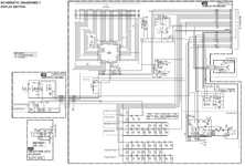
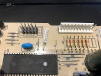
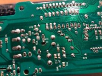
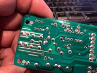
If you look at circuit boards from televisions , kitchen appliances , camcorders, audio equipment like harman kardon, onkyo etc . They have a distinctive 'look'. Many of these boards have special features. for example : many power supply and audio boards are single sided and use stitched wire bridges so the software needs to have provisions for that ( you are not going to drop wire bridges in schematics as parts , the pcb layout editor needs to do that on the fly, yet be able to export x-y coordinates so the pick and place machine can bend a piece of wire and shoot it , so length , rotation x,y needs to be exported. ) Same for the pcb's used in many switching power supplies like for pc and laptops. These all have very distinctive looks when it comes to routing style , island formation , pad formation etc.

So my question is : what do these guys use as pcb cad software. It is not going to be the usual suspects like cadence or mentor or altium or zuken. It may not even run on pc but be solaris/unix based. ( i know of a many esoteric systems like Bentley , Visula, Racal-Redac, Daisy systems, Vanguard (many european tv boards were made on that) SciCards, EMC and others but they all have been 'borged' by others)
So i am interested to see what tv makers like samsung, lg , sony use.. or companies like astec and antec , or harman kardon , onkyo , denon and others. Just look at service manuals from onkyo and clarion for example and look at those pcb layouts. Same thing if you take a camcorder from sony or canon apart. That is a very distinctive style. With boards that can be broken apart after soldering to mount them in the chassis. Even the wire harnesses are soldered before they break the boards apart.

So, who knows ? and who actually is using these tools ?
 

Hi,

The "look" is just cheap asian production style.
It can be done with almost any PCB layout software.

One could setup the autorouter parameters to generate just "linear jumer"... then optimize them manually.
The output may be post processed to get the "jumper data".

This is not my style. My PCB layouts are not that cost critical, mainly high reliable industrial design.

Klaus
Not true. Have you ever seen designs made by Cr5000 or ESD or Vanguard ? Those tools have special abilities you will not find in cadence/mentor/altium. Vanguard allows (allowed. that tool dates back to 1988 on the first 386 computers running under a proprietary operating system (it wasn't dos, but was a standard compaq 386 pc) you to stitch wire jumpers directly in the pcb without impacting netlist. The jumpers were exported in the pick and place data. I used that software at Nokia. Was made by Teradyne ). These tools have distinctive looks in their layout. You can immediately tell by looking at a pcb : that's made with that particular tool ( font type , style of trace termination , offset holes in pads (this was before teardropping) . ESD ran on solaris and was made to do hybrid design ( printed resistors and capacitors on ceramic substrate with naked silicon and bondwires . or BGA substrates. That too has special functionality not found in your average pcb design tool. Chip on board or chip on flex with pillars or bondwires. Here you need to be able to export bonding coordinates.) Many TV's in europe (Barco, Loewe, ITT) were designed on intergraph workstations using Clipper processors (all proprietary stuff) .

My quest is to find out what all tools are still out there. A lot of these tools are gone , but there is still stuff out there in daily use.
 

Hi,

If you say so...

When someone asks me to work with those tools I feel drawn back some decades.
Nowadays we have all the HF around: cellular phone, WiFi, Bluetooth....
It will be hard to make a EMI/EMC compatible PCB layout with one side copper and those jumper wires.
40 years, it maybe was good standard.

I did not say one find the exact tools in a modern PCB software.
But still one can do it with the modern tools.

Klaus
ok, you clearly do not understand my question.
It is not about high speed 24 layer boards with blind and buried via's. Cadence/ mentor/altium , been there done that. Been doing that for 23 years.

What i am looking for are year 2021 tools that are used in the far east to create white good / brown good products. Those product all use stamped , single sided boards with lots of wire bridges and thru-hole / smd mixed layouts. The software used for such designs has special abilities , like being able to create the wire stitches , being able to partition a sheet into multiple physically independent boards that will be collated using mouse bites into a panel. We're not talking repetitions of the same board but a puzzle-like approach where , after soldering, the board snaps into pieces for mounting in chassis of an audio amplifier. The schematic tools allow to tie boards using wire harnesses and propagate nets. in a traditional tool if you try to break a net named GND between two boards you will get an error that there is a broken connection. These tools allow to specify the connection is made through a wire harness. Zuken has some really specialistic capabilities to that end.

These tools will have special functions to do the panelisation / mousebite creation , printed carbon traces , and other stuff. that is what i am after. Whihc software tools are used for that. yes you can do it in cadence but it is a humongous manual job to try to shoehorn these features in. The tools i am talking about have those features.

Even their schematics have a special look and abilities that i cannot find in the usual tools. see the attached image. this is a single page describing 4 boards that are interconnected. they all together form 1 panel that can be broken. connections between boards are made by wire harnesses. if you look at the netnames : they are the same on both sides. a normal layout tool will tell you : broken net. Somehow this schematic tool 'understands' the connection goes through a physical wire and not a trace on the pcb.

the symbol and drawing style is not like the tools we know (cadence/mentor/altium) it is very unique. you can compare schematics from sony , onkyo , denon, and others. the drawing style is similar and highly deviating from 'western' tools.

So, question again : what is the name of these programs ? Anyone here work for samsung , LG, sony, onkyo as a pcb designer ? anyone here design circuits boards for lcd monitors, computer power supplies, wall-warts, tv's, refrigerators, air conditioners and the likes. What do you use ? I strongly suspect a lot of that software is japanese / korean in origin and only available over there with a user interface in japanese or korean. I want to know the name of the tool and the company that makes it and their website.

This is purely to satisfy my curiosity.
 

Attachments

  • s1.png
    s1.png
    275.6 KB · Views: 217

ok, you clearly do not understand my question.
It is not about high speed 24 layer boards with blind and buried via's.
Hi,

I did not write about designing a 24 layer board with blind and buried vias...
So please stay polite.

And surely I did understand your question.

What you don't understand is: It does not matter what board you design, even if it is a single layer low frequency board, with or without digital part, it needs to fulfill HF EMI/EMC standards. Simply because nowadays it is very likely that there is a HF source (cellular phone, etc ) nearby.
This is what I wrote.

Klaus
 

I see your point about multiple boards in a schematic page. Are you sure that the shown schematic is actually the primary design document of a multi board project? It might be a dedicated compilation for the service manual.

Of course, if there's a strong request to handle multi board projects this way, tool vendors may support it. I'm definitely not in a business with this need, but I'm interested to hear about this stuff.

Features discussed above like single layer autorouting with automatic jumper placement has been and is probably still supported by some industry standard tools. I never used it in an actual design, but I looked at it many years ago when comparing autorouter capabilities.
 

Hi,

I did not write about designing a 24 layer board with blind and buried vias...
So please stay polite.

And surely I did understand your question.

What you don't understand is: It does not matter what board you design, even if it is a single layer low frequency board, with or without digital part, it needs to fulfill HF EMI/EMC standards. Simply because nowadays it is very likely that there is a HF source (cellular phone, etc ) nearby.
This is what I wrote.

Klaus
True, but that does not preclude the usage of single layer boards. Go take a look at consumer products. many are using single layer boards. Take apart a microwave, refrigerator, lcd tv, 5.1 amplifier , you will find many single sided boards, all designed in the last 6 months. all using the techniques i described.
I am looking for the software that was used to make those. What is samsung, sony, onky, denon , jvc and all the asian guys using to do board design ?
The 'look' of layout and schematics is very different from 'western' cad tools.

I found a couple in the meantime
Zuken CR8000
Zuken Cr5000
Quadcept
Yokogawa Cadvance Alpha-III ( end of life end of 2020 -> bought out by zuken and killed off)
Sohwa-Sophia
PCAD Master Designer ( apparently NOT the P-CAD that was bought by Altium, it has a japanese user interface)
Unicraft OPUSER
CADLUS One www.cadlus.com
FIRST https://www.first-cad.com/products1/products1_top__en.html <-this one looks very interesting as it can do codesign of asic, substrates, wirebond, chp on board and board and trace the nets through all the elements.
 

True, but that does not preclude the usage of single layer boards. Go take a look at consumer products. many are using single layer boards
I did not say so.
I said "It's hard" and this is how I meant it.

With other discussions about PCB layout - especially for unexperienced members - I say that it's easier to create a "EMI/EMC good" PCB layout as 4 layer than with 2 layers. For a good 2 layer PCB you need more experience.

And for sure the companies you talk about - they have experience. And they include the metal case into consideration. They know how to go to the limits.
A couple of years ago I was at an EMI/EMC test house with one of my designs.
The result was that my design (switch mode power supply, about 10W) was about 40 dB below the limit (bare PCB, no shielding).
I asked about the result of other companies' design. He told me that he just had tested a comparable SMPS of a big international SMPS manufacturer. It was just 3dB below the limits although it hat a metal case. I'm sure they know what they do... just to fulfill the regulations with lowest part cost.

Klaus
I know.. but then mass produced products are penny pinching like anything. And they have to be. A couple of years ago i was called to the customer in Singapore to help solve an EMC problem (near field) with one of our devices (i used to design silicon for harddisks) . I solved it by 'tuning' the capacitors on the power rail so that they would form the lowest impedance on the frequency that was causing trouble. The design was above limit in a pretty narrow band, so i picked a couple of values that would dampen that band.

The answer: No we can't do that as it would increase the product cost.
Wait ? You mean the bom cost ? No, the new values are same price, or cheaper, i checked that.
No sir, the product cost. You see, the robots now install 1 component type. This now goes to 3 component types. The logistics involved in warehouse for three parts vs 1 part , and the fact that the robot needs to change nozzles 1 extra time ( the bulk caps were three 0402, i changed that to one 0402 and two 0201. A nozzle change was required between 0402 and 0201), they would need another machine as there were not enough feeder slots free... all that stuff drove the price slightly over 2 dollar cent in production overhead (not bom overhead). Pr drive.

What's 2 cents ? Well this particular drive was a high runner (laptop drive).. they build about 800.000 PER DAY ... that was 5 million dollar per year in overhead... not an acceptable change !

I ultimately solved it by altering the control loop of the switching regulator to push his noise into the band where we were allowed a higher level, and tweaking the PCB layout in terms of via placement. There too they were picky... an additional via costs additional time and drill bit wear... i managed to shorten one loop by shuffling some stuff around without requiring an additional via.

These things are not easy.

For lots of household stuff they are fortunate to have metal enclosures. Without that none of their stuff would pass. You even have to be careful with the screws holding them together. They are of such crappy quality that if you open and close the enclosure a coupe of times the threads ( and the sheet metal itself) wear out enough that you get field leakage there.

And multilayer boards are not always the answer. When i was at Alcatel we had an issue with a DSLAM ( Digital Subscriber line Access Mulitplexer, if you have ADSL or VDSL for your internet over phone line: the box that sits on the other side feeding data to all the customers. big 24 inch wide racks in rows in airconditioned buildings.)
All was fine, until they installed the uart board. That board had nothing except some SC68 series UART from philips (now NXP) , a crystal and a couple of capacitors and a db-9 port. Only used so they could hook up a row controller to do firmware updates. (Most updates were done over the ATM backplane , but an update to the bootrom required going in through a serial port. You needed to stop the OS (a modified iRMX kernel) on the i960, throw it in uart mode (that code was a hard ROM in the silicon and would always work, even if you lost the main flash) and do the patch. All this could be done remotely . These systems are always-on ( when is the last time you heard a telephone exchange crashed ... never. Doesn't happen.) Anyway , i deviate

All these boards are a standard size to fit in the cage. They made a 4 layer board with the parts neatly spaced together signal , ground, power, signal , with the bottom signal flooded with ground as well. The whole thing radiated like a dipole antenna. A harmonic of the crystal frequency was apparently nicely resonant with the power/ground plane and it edge radiated like hell. This was the only card that had ... a plastic front cover , as opposed to the metal covers for the line cards. Solution: a couple of 10nF capacitors at the edge of the board to 'shunt' the planes. They did not want to remove the empty copper as that would load the etching baths too much. a capacitor shunt was cheaper. So if you ever see a large board with few parts on it , that has , what looks like a decoupling capacitor, all the way at the opposite edge of the board : that's there to shunt the dipole formed by the planes in the board.

My curiosity into these asian cad tools is not for these kind of purposes (emc , multilayer etc) . I am after the 'special' sauce they have to do things like wire straps, carbon traces for membranes , breakable and bonded boards etc. Sure you can do that with cadence and altium but it is a pain and a lot of manual work.

Those tools ( like Zuken) have special functions that solve that in an automated way saving lots of time. I'd like to see how these tools work and how they solved that so i can port it to my tools library. Mouse bites for example , i have a script where i draw the parting line between two board sections and it creates the structures on the fly. If i alter the board shape later i can rebuild all the mouse bites with one click. Altium can do wire stitching for single layer boards , but it cannot export the coordinates. And it will let you stitch things that are 'impossible' like bent wires. Furthermore , you want these stitches to be a fixed length so the robot does not have to create random lengths.

See the pictures below for an idea of what i am talking about. The cad tool knows that this is not a broken net and that this particular line has to become a 'component' in the BOM ( the wire ) , in the pick and place file (x,y,length and rotation) , but does not go back to the schematic as 'component' . Cadence/mentor/Altium do not have these capabilities (not in a fully automated way) . So my question is : what cad tool was used to do this board ? Look at the routing on the backside. That is a very distinctive 'look' . Offset holes in oblong pads . Solder strips in high current areas. Yes you can do this by hand, but i strongly suspect those programs have 'tools' where you draw an area and tell them : i need solder stripes here , this wide, this pitch, and the program floods the area, automatically avoiding existing holes.

I don't believe that such things are done by hand line by line. Not in 2021... (this board was made about a year ago) There has to be cad software that has these features built in. And i heavily suspect it is asian cad software due to the prevalence of such board designs 'over there'. I want to find out what those programs are and see how they work to learn new tricks that i can port to my script library to bolt it on to my toolchain.
 

Attachments

  • q1.jpg
    q1.jpg
    75.8 KB · Views: 184
  • q2.jpg
    q2.jpg
    106.3 KB · Views: 191
  • q3.jpg
    q3.jpg
    98.9 KB · Views: 225
Last edited:

Hi,

I´ve known from the beginning what you mean.

Please note: I don´t tell you that you need to use software x, nor do I know the name of a software with these feature.

All I´m sayingis: it can be done with standard software and a bit of post processing.
Just for me speaking ( no need that you do the same).
I´d use a standard routing layer ... tell the autorouter (indeed I very rarely use an autorouter) just to use horizontal or vertical traces ...and use solderable pads instead of the usual wires (maybe this can be done by the post processing).
Then some kind of post processing this special layer.

I never will have this layer "produced" on the PCB. But the layer data tells me where to place a jumper wire and it´s length.
For me it´s not much of a difference whether there are traces with a via at each end in an inner layer ... or there are jumper wires on a one sided board.
The handling of the tool is the major difference.

I know it will not be exactly how you want it to work or what you want to hear.

Klaus
 

Most of the methods mentioned I have been able to do in Cadstar by Zuken, including the wire stitching as you call it (Cadstar calls them jumpers).
However I am sure that all these manufacturers are not using Cadstar, ISTR Philips did.
They change their tools from time to time (retaining a seat of the old one for maintenence etc.) usually so that they can get certain features not had before.

Many features can still be done even if it is not a natural feature of the tool, there are workarounds that can be done - put the time into coming up with a method and it can become quick and easy to do. I was doing the wire stitching before Zuken included it as a feature by simply making a part with multiple alternatives for different lengths.

As for exporting the wire information, well that's easy enough to write into the part information which can then be output in the files.

Still it would be good to know what they use if you ever find out.
 

Status
Not open for further replies.

Part and Inventory Search

Welcome to EDABoard.com

Sponsor

Back
Top