Continue to Site

Welcome to EDAboard.com

Welcome to our site! EDAboard.com is an international Electronics Discussion Forum focused on EDA software, circuits, schematics, books, theory, papers, asic, pld, 8051, DSP, Network, RF, Analog Design, PCB, Service Manuals... and a whole lot more! To participate you need to register. Registration is free. Click here to register now.

vhdl code for an octal d-type flip flop register with clock enable

Status
Not open for further replies.

krisdan

Banned
Joined
Oct 17, 2014
Messages
4
Helped
0
Reputation
0
Reaction score
0
Trophy points
1
Activity points
0
good *** gurus in the house... can anyone help me with the vhdl code for an octal d-type flip flops with clock enable? thanks waiting for your urgent replies....
 

Can u try doing it yourself? It is pretty simple. Do it for 1 flop and and then replicate it 8 times...You will get the logic diagrams easily from the net..
 

It is a classic example:


Code VHDL - [expand]
1
2
3
4
5
6
7
8
9
10
11
12
13
14
15
16
17
18
architecture example of reg4 is
begin
    storage : process is
        variable v0, v1, v2, v3 : bit;
    begin
        wait until clk = '1';
        if en = '1' then
            v0 := d0;
            v1 := d1;
            v2 := d2;
            v3 := d3;
        end if;
            q0 <= v0 after 5 ns;
            q1 <= v1 after 5 ns;
            q2 <= v2 after 5 ns;
            q3 <= v3 after 5 ns;
    end process storage;
end architecture example ;


thanks for the response but is dt for d octal d type flip flop with clock enable cos am only seeing a q0 to q3......
i also need the testbench too if possible.....thnx in advance


av sent a pdf file which contails the truth table....can u pls help me to look at it?
 

Attachments

  • SN74HC377.pdf
    239.5 KB · Views: 70
Last edited:

It is a classic example:


Code VHDL - [expand]
1
2
3
4
5
6
7
8
9
10
11
12
13
14
15
16
17
18
19
20
21
22
23
24
25
26
27
28
29
30
31
entity reg8 is
    port ( d0, d1, d2, d3, d4, d5, d6, d7, en, clk : in bit;
    q0, q1, q2, q3, q4, q5, q6, q7 : out bit );
end entity reg8 ;
 
architecture example of reg8 is
begin
    storage : process is
        variable v0, v1, v2, v3, v4, v5, v6, v7 : bit;
    begin
        wait until clk = '1';
        if en = '1' then
            v0 := d0;
            v1 := d1;
            v2 := d2;
            v3 := d3;
            v4 := d4;
            v5 := d5;
            v6 := d6;
            v7 := d7;
        end if;
        q0 <= v0 after 5 ns;
        q1 <= v1 after 5 ns;
        q2 <= v2 after 5 ns;
        q3 <= v3 after 5 ns;
        q4 <= v4 after 5 ns;
        q5 <= v5 after 5 ns;
        q6 <= v6 after 5 ns;
        q7 <= v7 after 5 ns;
    end process storage;
end architecture example ;

 
Last edited:

thanks i rili appreciate it.. what of the test bench
 

It is obvious that this is a school homework, so I would not normally answer, but I think the previous answers are confusing for a beginner.
Maybe the school wants you to design a single bit d-type flip flop and then instantiate it 8 times.
That is not how we do it in the real engineering world, but the core function will look like this, regardless of the number of bits:


Code VHDL - [expand]
1
2
3
4
5
6
7
8
process(clk)
begin
  if rising_edge(clk) then
    if clock_enable = '1' then
      data_out <= data_in;
    end if;
  end if;
end process;


where data_in and data_out can be single bits or vectors of any size.

The rest of the code and the test bench is up to you. You will learn nothing if we give you the answer here. Use your VHDL book and Google to collect the information you need.
 
I would suggest using the following coding of an octal d-flip flop with enable:

Code VHDL - [expand]
1
2
3
4
5
6
7
8
9
10
11
12
13
14
15
16
17
18
19
20
21
22
23
24
library ieee;
use ieee.std_logic_1164.all;
 
entity octal_dffe is
  port (
    q   : out std_logic_vector (7 downto 0);
    d   : in  std_logic_vector (7 downto 0);
    clk : in std_logic
  );
end entity octal_dffe;
 
architecture example of octal_dffe is
begin
 
  dffe : process (clk)
  begin
    if rising_edge (clk) then
      if (en = '1') then
        q <= d;
      end if;
    end if;
  end process dffe;
 
end architecture example;


If someone presented me with the "classic" method of writing a octal D-FF in an interview I wouldn't hire them.

- - - Updated - - -

It is obvious that this is a school homework, so I would not normally answer, but I think the previous answers are confusing for a beginner.
Maybe the school wants you to design a single bit d-type flip flop and then instantiate it 8 times.
That is not how we do it in the real engineering world, but the core function will look like this, regardless of the number of bits:
This was the reason why I answered with what would be done by real world engineers. Along with my comment about not hiring anyone who would write something like the code in #3 and #4.

The rest of the code and the test bench is up to you. You will learn nothing if we give you the answer here. Use your VHDL book and Google to collect the information you need.
Unfortunately given the lack of quality in the code snippets "out in the wild" they are likely to continue the trend of antiquated coding styles (the education system also seems to be behind the times based on the plethora of pre-2000 coding styles being used for both VHDL and Verilog.

My suggestion to the OP is read the VHDL 2008 LRM (I know I've stated I'm too lazy and cheap to read or buy it...but then I'd rather code in Verilog ;-)) even relatively recent releases like the 2nd Ed of Pedroni's book still use some antiquated code like clk = '1' and clk'event instead of rising_edge(clk) at least that book doesn't push using the non-standard packages std_logic_arith, std_logic_unsigned,... etc.
 
hello

please I need help in VHDl code Hex d flip flops with clear and testbench as well..... thanks
 

hello

please I need help in VHDl code Hex d flip flops with clear and testbench as well..... thanks

You should be able to extrapolate how to write a hex D-FF with clear instead of an enable from post #6 or #7. If you can't then you could perform a search on google.
 

Sorry.... I tried many times, but I could not could you help me please.
 

To be honest, I am a beginner in VHDl

This is the table of HEX D flip flops with clear

I do not understand it exactly

View attachment 110732
 

There is no attachment. I'm assuming that you tried to upload a picture of the truth table for a D flip flop with clear. As you seem to be unclear what the D flip-flop truth table describes, I suspect you need to learn more about digital logic than learning VHDL. For the D flip-flop with clear you can study this tutorial:

https://www.electronics-tutorials.ws/sequential/seq_4.html
The up arrow and down arrow represent the clock transition from a low to high and a high to low respectively.

Besides that tutorial you might want to take a look at their boolean algebra, binary numbers, and other sections.

Now if you still want a code example (spoiler alert!)...
Using google with the search terms: "vhdl d flip flop with reset" you should get this link near the top:
Code:
http://www.asic-world.com/examples/vhdl/d_ff.html
(note: I'm specifically making this link none clickable in the hopes that you will try performing the search yourself on google using the given search terms, since the use of LMGTFY links seem to be currently frowned upon :cry:)

Examine the example code on that asic-world link and compare it to the enable code given in both #6 & #7. You should be able to recognize why you can extrapolate the clear version from the enable version. If not then you probably need to study the LRM and/or a VHDL book and really learn the syntax of the language instead of just looking at a bunch of code snippets on the internet.
 

74)this is the function table (SN74)

inputs output
____
clear clock D Q
L X X L
H rising edge H H
H rising edge L L
L L X Q0
 

the last line is
____
clear L
clock X
D X

And Q Output is c Q0

............inputs..................................output
clear................clock............... D............Q

L ......................X...................X............L
H..................rising edge...........H............H
H..................rising edge...........L.............L
L.......................L...................X............Q0
 

There is no Clear input only C enable low.
image.jpg
 

not the same

please click on this

dff.PNG
 

I mean HEX D flip flops with clear.... not d-type flip flop register with clock enable not the same
 

No idea who originates the table in your post, but it's definitely wrong, because line 1 and line 4 are mutually exclusive. Wrong clear polarity.

Please compare with an original xx74 document:
1433599300_1414330714.jpg


I mean HEX D flip flops with clear.... not d-type flip flop register with clock enable not the same.
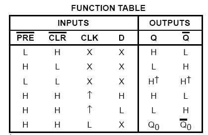
Yes. I'm completely with ads-ee in this regard
You should be able to extrapolate how to write a hex D-FF with clear instead of an enable from post #6 or #7. If you can't then you could perform a search on google.
 

Status
Not open for further replies.

Similar threads

Part and Inventory Search

Welcome to EDABoard.com

Sponsor

Back
Top