Continue to Site

Welcome to EDAboard.com

Welcome to our site! EDAboard.com is an international Electronics Discussion Forum focused on EDA software, circuits, schematics, books, theory, papers, asic, pld, 8051, DSP, Network, RF, Analog Design, PCB, Service Manuals... and a whole lot more! To participate you need to register. Registration is free. Click here to register now.

Very simple SPI Slave with VHDL (But have not worked)

Status
Not open for further replies.

sakti_boy

Newbie level 4
Joined
Aug 29, 2012
Messages
7
Helped
0
Reputation
0
Reaction score
0
Trophy points
1,281
Activity points
1,394
Hallo,

I am quiet new with VHDL programming language.
Now, I make an FPGA as SPI Slave, and microcontroller as SPI Master.

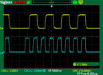
This Picture is the SPI Master from the microcontroller
(just normal SPI, without ChipSelect)
Yellow is the MOSI (0x55)
Blue is SCLK
spimaster.png


FPGA receive the signal from SCLK and MOSI of microcontroller,
Here is my VHDL Program

-----------------------------------------------------------
-----------------------------------------------------------
LIBRARY ieee;
USE ieee.std_logic_1164.all;
USE ieee.std_logic_arith.all;
USE ieee.std_logic_unsigned.all;

ENTITY spi_slave IS
GENERIC(
d_width : INTEGER := 8; --data bus width (8bit)

sclk1 : IN STD_LOGIC; --spi clk from master
mosi1 : IN STD_LOGIC; --master out, slave in
rx_data1 : OUT STD_LOGIC_VECTOR(d_width-1 DOWNTO 0);
END spi_slave;

ARCHITECTURE logic OF spi_slave IS

SIGNAL toggle : INTEGER RANGE 0 TO d_width := 0;
SIGNAL rx_buff1 : STD_LOGIC_VECTOR(d_width-1 DOWNTO 0) := (OTHERS => '0');

BEGIN
PROCESS(sclk1,toggle)
BEGIN
IF(rising_edge(sclk1)) THEN --rising edge, then capture the mosi
rx_buff1 <= rx_buff1(rx_buff1'left - 1 downto 0) & mosi1; -- capture mosi into rxbuff1
toggle <= toggle +1; --toggle as counter (8bit data received)
IF (toggle = 8) THEN --if toggle goes 8, then reset, and fill the output rx_data1 with rx_buff1
rx_data1 <= rx_buff1;
toggle <= 0;
END IF;
END IF;
END PROCESS;
END logic;

However, it did not really work.
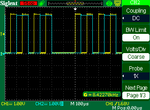
Each output pin rx_data1, always goes high and low one after another, although I send always the same data 0x55
I think each pin will goes always low for the 0, and high for the 1, because the data is always the same.

The pin which should be 1 and 0, goes high and low in different phase ( I think, fpga can capture the spi master, there might be wrong with shifting)
you can see picture here
outputpin.png

it seems that every pins goes high and low, with next shifting measurement.
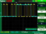
In this picture below,
yellow is mosi.
blue is one of output pin.
mosi_outputpin.png
one of output (rx_data1) toggles on the next sequence of mosi input.

I have not implemented Chip Select, because my input pin of CS cannot detect the signal correctly,
but I think without CS, it will still work. (only one slave)
I have already spent several weeks, but it still the same. I am really stuck

Is there any one have this kind of experience before ?
or Maybe anyone know what is wrong with my program ?

Any helps, suggestions will be very appreciated.

Thanks in advance
 

PROCESS(sclk1,toggle)
BEGIN
IF(rising_edge(sclk1)) THEN --rising edge, then capture the mosi
rx_buff1 <= rx_buff1(rx_buff1'left - 1 downto 0) & mosi1; -- capture mosi into rxbuff1
toggle <= toggle +1; --toggle as counter (8bit data received)
IF (toggle = 8) THEN --if toggle goes 8, then reset, and fill the output rx_data1 with rx_buff1
rx_data1 <= rx_buff1;
toggle <= 0;
END IF;
END IF;
END PROCESS;

Your toggle signal is cycling over 9 sclks as you start at 0 and count until it reaches 8. I'm not expert in VHDL but I would code the counter as:


Code VHDL - [expand]
1
2
3
4
5
IF (toggle = 7 ) THEN
  toggle <= 0;
ELSE
  toggle <= toggle + 1;
END IF;


not sure how VHDL treats the counter outside the IF (toogle = 8) when the reset is buried inside that IF statement.


Regards,
-alan
 
I'm no vhdl person either, but this ...


Code VHDL - [expand]
1
IF(rising_edge(sclk1)) THEN --rising edge, then capture the mosi


Would mean that you are using the SCLK input as a clock input. As in taking up a global clock net. In principle you can do that, run the spi slave synchronous to the external clock if that's what you want. As long as you don't forget to put a synchronizer / fifo between that spi slave and the rest of your system...

Personally I'd run the spi slave on an fpga internal system clock and oversample the SCLK + MOSI line...
 
Personally I'd run the spi slave on an fpga internal system clock and oversample the SCLK + MOSI line...

Good advice, unless your FPGA's SPI needs to be up and running to bridge the SPI to the clock synthesizer chip that has to be programmed at startup.

It's always nice to have a design with only one clock domain, but that is a luxury that I haven't had for a long time. :cry:

Regards,
-alan
 

Good point. :) It's just that based on "I am quiet new with VHDL programming language" from the OP I was guessing that this may have not been entirely intentional. Especially if he extrapolates that coding habit of rising_edge(some_random_signal) to all code that might be a tad problematic. ;) rising_edge of a real clock, yes. rising_edge of a generic signal, best not if you want your code to be synthesizable. There even was a thread about that recently...
 

Hi all,

thanks for your help. :)
I have already tried both of the cases.

but it is still not working properly.
each pins are still toggling high and low.
the different is only the period, it toggles with very slow frequency, less than 10Hz (my SPI master send data 10kHz)
However, this spi slave(Fpga) is not accurate then, how can it receive the data, if the data always toggle high and low ?
I mean, it does not know which pin is actually low or high.
 

I suggest running the FPGA at a much higher frequency (say 10 Mhz) and just treating the SPI clock as another signal. Make sure you synchronise everything properly and it should work fine. Ive done this very successfully with a 300MHz system clock and SPI clock of 20MHz.
 

As I just started a long synthesis/build and was curious I tried compiling the op's posted code:

Well surprise it doesn't even compile in Modelsim. So I fixed the compile errors and changed to cycle on toggle = 7 (otherwise the design doesn't even work as toggle can reach a value of 9 which is invalid). Even then the rx_buff1 capture is done wrong as it tries to capture the shifted data at the 7th bit shift instead of the 8th bit. So I fixed that too and ended up with the following simulation result:

spi.GIF

Well it works as long as one doesn't mind having to perform a dummy byte transfer to get the rx_data1 register loaded.

Can't believe the op is testing this code in HW, as it won't even compile!

Regards,
-alan

- - - Updated - - -

As I just started a long synthesis/build and was curious I tried compiling the op's posted code:

Well surprise it doesn't even compile in Modelsim. So I fixed the compile errors and changed to cycle on toggle = 7 (otherwise the design doesn't even work as toggle can reach a value of 9 which is invalid). Even then the rx_buff1 capture is done wrong as it tries to capture the shifted data at the 7th bit shift instead of the 8th bit. So I fixed that too and ended up with the following simulation result:

spi.GIF

Well it works as long as one doesn't mind having to perform a dummy byte transfer to get the rx_data1 register loaded.

Can't believe the op is testing this code in HW, as it won't even compile!

Regards,
-alan
 

Hello,

the problem is solved, :D
I add another signal to tunnel the Input logic, I think it is because of my lack basic about vhdl.
Heh ? I run the program with Quartus 2 12 sp1 web edition, it can be compiled.

Thanks everyone.
 

Hello,
I run the program with Quartus 2 12 sp1 web edition, it can be compiled.

I copied the code in the first post and put it in a file called test.vhd and did vcom test.vhd in Modelsim and get the following error:

# Model Technology ModelSim SE-64 vcom 10.1b Compiler 2012.04 Apr 26 2012
# -- Loading package STANDARD
# -- Loading package TEXTIO
# -- Loading package std_logic_1164
# -- Loading package std_logic_arith
# -- Loading package STD_LOGIC_UNSIGNED
# -- Compiling entity spi_slave
# ** Error: test.vhd(12): Object 'd_width' cannot be used within the same interface in which it is declared.
# ** Error: test.vhd(12): Bad expression in left bound of range expression.
# ** Error: test.vhd(12): Type error in range expression.
# ** Error: test.vhd(13): near "END": expecting FUNCTION or PROCEDURE or IMPURE or PURE
# C:/modeltech64_10.1b/win64/vcom failed.


Sure looks like compile problem to me. The generic isn't even ended with a ')' so it's definitely not correct in your original post.


Regards,
-alan
 

hi alan

I am so sorry, make you confuse.
It is my fault, I make mistake in copying the code.
my original copy has so many comments to erase my previous trial of code, so i have to copy here one by one.
Thus, some of it was not correct, but the main idea of program was fine

I copy here again, it should be compiled.

LIBRARY ieee;
USE ieee.std_logic_1164.all;
USE ieee.std_logic_arith.all;
USE ieee.std_logic_unsigned.all;

ENTITY spi_master IS
GENERIC(
d_width : INTEGER := 8); --data bus width


PORT(
clk1 : IN STD_LOGIC; --spi clk from master
sclk1 : IN STD_LOGIC; --spi clk from master
ss_n1 : IN STD_LOGIC; --active low slave select
mosi1 : IN STD_LOGIC; --master out, slave in
rx_data1 : BUFFER STD_LOGIC_VECTOR(d_width-1 DOWNTO 0));-- := (OTHERS => '0')); --receive register output to logic

END spi_master;

ARCHITECTURE logic OF spi_master IS

SIGNAL toggle : INTEGER RANGE 0 TO d_width-1 := 0; --count spi clock toggles
SIGNAL mode1 : STD_LOGIC; --groups modes by clock polarity relation to data
SIGNAL bit_cnt1 : STD_LOGIC_VECTOR(d_width DOWNTO 0); --'1' for active transaction bit
SIGNAL rx_buff1 : STD_LOGIC_VECTOR(d_width-1 DOWNTO 0) := (OTHERS => '0'); --receiver buffer

BEGIN
PROCESS(clk1, sclk1,toggle)
BEGIN
IF((clk1 = '0') OR (clk1 = '1')) THEN
IF(rising_edge(sclk1)) THEN
rx_buff1 <= rx_buff1(rx_buff1'left - 1 downto 0) & mosi1;
IF (toggle = 7) THEN
rx_data1 <= rx_buff1;
toggle <= 0;
ELSE
toggle <= toggle +1;

END IF;
END IF;
END IF;
END PROCESS;
END logic;
 

The VHDL code for the SPI slave is even simpler if you use the slave select pin from the SPI master instead of trying to count the clock pulses. **broken link removed** contains two VHDL examples.
 

The VHDL code for the SPI slave is even simpler if you use the slave select pin from the SPI master instead of trying to count the clock pulses.

Potentially interesting but could you be more specific?

Related to the use of a slave select (CS) signal ... sometimes you don't want to use a CS because 1) there's only a single SPI slave and 2) you want to reduce the number of pins required.
 
Potentially interesting but could you be more specific?

Related to the use of a slave select (CS) signal ... sometimes you don't want to use a CS because 1) there's only a single SPI slave and 2) you want to reduce the number of pins required.

The article that I linked to talks about the micro and SPI slave (on CPLD) possibly going out of sync when only the clock and data lines are used. When the micro starts up it could put a clock pulse on the SPI slave and the SPI slave will then clock in one bit. When the real data byte is sent over SPI, only the first 7 bits will be clocked in.

Not much space in that CPLD for implementing a timing mechanism for resetting the the clock pulse counter. Any ideas for a solution to stop the sync problem only using clock and data lines of the SPI port?
 

A yes, that problem. :)

I must admit my brain was in fpga mode and not cpld mode. Lack of FFs is not really an issue on fpga. But interesting problem...

You want to implement a timeout mechanism on the SPI slave (the cpld). The main reason to not use a CS signal is to save 1 wire between cpld and mcu, and also you don't want to tie up an IO on the mcu side since that might be a scarce resource.

Two methods I can think of (there are probably more ;):
1 - by using a clever implementation of several co-prime counters + clock enabling. The main drawback of this is: takes too much typing to explain. And as such, numero duo:
2 - cheat! redefine the problem such that you still do NOT want to use a wire between cpld and mcu, nor a pin on the mcu. However using a pin on the cpld is fine.

After all, FFs are scarce on cpld but pins are not. So use an external R + C for your timing. Depending on the IO capabilities of your cpld you need 1 or 2 pins. In the optimal case you can do the charging, comparing and discharging all with the same IO. If not use 2 pins for charge/discharge (output) and comparator (input).

This is assuming that you don't really care if the timeout is for example 1 ms or 1.5 ms, but that seems reasonable enough for this type of problem.
 

A synchronous interface without slave select can work, but doesn't deserve the name SPI.

The solution suggested by mrflibble promises minimal digital resource requirement.
 

A yes, that problem. :)

I must admit my brain was in fpga mode and not cpld mode. Lack of FFs is not really an issue on fpga. But interesting problem...

You want to implement a timeout mechanism on the SPI slave (the cpld). The main reason to not use a CS signal is to save 1 wire between cpld and mcu, and also you don't want to tie up an IO on the mcu side since that might be a scarce resource.

Two methods I can think of (there are probably more ;):
1 - by using a clever implementation of several co-prime counters + clock enabling. The main drawback of this is: takes too much typing to explain. And as such, numero duo:
2 - cheat! redefine the problem such that you still do NOT want to use a wire between cpld and mcu, nor a pin on the mcu. However using a pin on the cpld is fine.

After all, FFs are scarce on cpld but pins are not. So use an external R + C for your timing. Depending on the IO capabilities of your cpld you need 1 or 2 pins. In the optimal case you can do the charging, comparing and discharging all with the same IO. If not use 2 pins for charge/discharge (output) and comparator (input).

This is assuming that you don't really care if the timeout is for example 1 ms or 1.5 ms, but that seems reasonable enough for this type of problem.


I certainly hope I have a pin to spare, would not want to go to all that trouble 8-O, :wink:
 

Status
Not open for further replies.

Part and Inventory Search

Welcome to EDABoard.com

Sponsor

Back
Top