Continue to Site

Welcome to EDAboard.com

Welcome to our site! EDAboard.com is an international Electronics Discussion Forum focused on EDA software, circuits, schematics, books, theory, papers, asic, pld, 8051, DSP, Network, RF, Analog Design, PCB, Service Manuals... and a whole lot more! To participate you need to register. Registration is free. Click here to register now.

Tuning distributed elements on a PCB

Status
Not open for further replies.

wesmonty

Newbie level 6
Joined
May 15, 2018
Messages
12
Helped
0
Reputation
0
Reaction score
0
Trophy points
1
Activity points
181
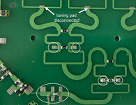
With lumped elements it's easy to tune the matching network on a PCB, one can just change the capacitor or inductor for a different one, but I'm wondering what the method is for tuning a PCB that uses distributed elements such as open circuit stubs, for example. Could anyone provide any advice on this subject please?

Cheers,
Wes
 

There is not so much option for that, but some open stubs can be tuned by adding extra length that is not connected yet, but they can be designed as connectable. Of course, this method is very limited, and it is applicable to appropriate pcb structures only.
The best method is to simulate the PCB with well-defined substrate parameters and surely with good modelled discrete components. There may be slight shifts but there isn't any other option.
 

    wesmonty

    Points: 2
    Helpful Answer Positive Rating
basically you use capacitive tuning.
lets say there is an open circuited microstrip stub. You take some copper ribbon, maybe 20 mils wide, make a 20x40 square of it, take a cut end of a wooden qtip, add someting sticky to it, and stick the copper to the end of the wood handle. then take the copper rectangle and move it around on the microstrip trace. when you find the best position to tune your circuit, you solder it on in that location
 

    wesmonty

    Points: 2
    Helpful Answer Positive Rating
Thanks, both. Would it be correct to say that a properly simulated design would generally not need any tuning of distributed elements?
 

Thanks, both. Would it be correct to say that a properly simulated design would generally not need any tuning of distributed elements?
Nah, Every RF circuit needs a tuning. More or less.
Also depends on your specifications, loose or tight
 

Nah, Every RF circuit needs a tuning. More or less.
Also depends on your specifications, loose or tight
Interesting as I've never come across anything in literature about tuning like this, although maybe I haven't looked hard enough. Could you point me to any general advice on this?
 

Thanks, both. Would it be correct to say that a properly simulated design would generally not need any tuning of distributed elements?
You can predict the passive components (layout + SMD) very accurately using EM simulation + circuit models, but for the active devices there might be some uncertainty. Tolerances are also an issue.

It really depends how critical/narrowband your design is. Having the extra tuning elements in layout that can be connected or cut off is a common solution if necessary.

Attached is a PCB photo from the 1990s where we used that method: we didn't have EM simulation at that time and isolation of the couplers was critical and required some tuning.
 

Attachments

  • tuningpads.jpg
    tuningpads.jpg
    133.5 KB · Views: 117

Status
Not open for further replies.

Part and Inventory Search

Welcome to EDABoard.com

Sponsor

Back
Top